Substrate and circuit board

A technology of circuit boards and substrates, which is applied to printed circuit components, circuit inspection/recognition, etc., can solve the problems of fading graphics, blurred positioning marks, and inability to provide references for electronic component deployment, so as to improve production levels and avoid The effect of inaccurate positioning and reducing production loss

Pending Publication Date: 2017-02-15
NUBIA TECHNOLOGY CO LTD
View PDF3 Cites 1 Cited by
  • Summary
  • Abstract
  • Description
  • Claims
  • Application Information

AI Technical Summary

Problems solved by technology

However, there is a disadvantage of the graphics and texts obtained by silk screen printing, that is, the printed graphics and texts are very easy to fade due to long-term wear and tear.
The positioning marks for electronic components are blurred, and it is impossible to provide reference for the deployment of electronic components in the later stage, resulting in inaccurate positioning of electronic components, and the problem that circuit boards have to be discarded as "waste products".

Method used


Image

  • Substrate and circuit board
  • Substrate and circuit board
  • Substrate and circuit board

Examples


no. 1 example

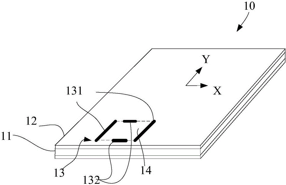
[0029] This embodiment provides a substrate, please refer to figure 1 , the substrate 10 includes a metal layer 11 and an ink layer 12 covering the surface of the metal layer 11 . Various types of electronic components can be deployed on the surface of the substrate 10 , such as capacitors, resistors, triodes, and other chip components that implement various functions. In order to locate certain components that need to be arranged on the substrate, positioning marks can be arranged on the surface of the substrate 10 .

[0030] The positioning mark in this embodiment is realized by etching the ink layer 12 on the metal layer 11 . Etching is the technique of removing material using chemical reaction or physical impact. Etching technology is a light-weight processing technology in PCB production, which can be divided into wet etching and dry etching. The basic principle is: the ink layer 12 is usually black or dark green. The metal layer 11 used in the substrate 10 is basical...

no. 2 example

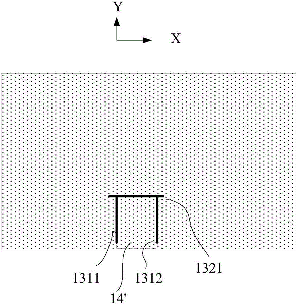
[0042] This embodiment will continue to introduce the substrate and the circuit board including the substrate. In order for those skilled in the art to understand the advantages and details of the substrate and the circuit board in this embodiment more clearly, the following combined Figure 6 To elaborate:

[0043] exist Figure 6 Among the substrates 60 provided, the positioning mark 63 arranged on the surface of the substrate still includes a first limit mark 631 for indicating the limit of the electronic component in the first direction, and a limit mark 631 for indicating that the electronic component is set in the second direction. Set the second limit mark 632 of the limit, and the first direction is perpendicular to the second direction. The first limit mark 631 is a line segment parallel to the second direction formed by etching the ink layer on the copper clad board; the second limit mark 632 is a line segment parallel to the first direction formed by etching the in...


PUM


Abstract

The present invention discloses a substrate and a circuit board. The substrate comprises a metal plate covered with an ink layer; the surface of the substrate is provided with a positioning mark formed by etching the ink layer on the metal plate, wherein the positioning mark can indicate the setting position of an electronic component to be set on the surface of the substrate. According to the substrate provided by the embodiments of the present invention, the positioning mark of the electronic component is a pattern formed by etching the ink layer covering the surface of the metal plate. According to a mode in the prior art, another material of which the color is different from an ink layer is adopted additionally to form a positioning mark, while, according to the substrate of the invention, the ink layer on the metal layer is removed, so that exposed metal can be adopted to form the positioning mark, and the positioning mark will not be abraded and faded, and therefore, the positioning mark can provide effective and reliable reference for the setting of the electronic component, and the problem of wrong setting of the electronic component caused by inaccurate positioning due to the fading of the positioning mark formed by screen printing can be avoided, production loss can be reduced, and the production level of the circuit board can be improved.

Description

technical field [0001] The invention relates to the field of communication equipment, and more specifically, to a substrate and a circuit board. Background technique [0002] There are circuit boards in various electronic devices, and various functional circuits and electronic components are deployed on the circuit boards to realize different functions and provide users with required services. Most of the existing circuit boards are PCB (Printed Circuit Board, printed circuit board) boards, and most of the circuit connections have been realized when the PCB board is printed and manufactured, but the components that need to be set in the circuit need to be reworked later. Fixed setting. The installation position of electronic components in the functional circuit is relatively fixed. After the PCB is manufactured, the installation position of the electronic components is also determined. Due to the powerful functions of today's electronic equipment, the circuits in the circu...

Claims


Application Information

Patent Timeline
Patent Type & Authority Applications(China)
IPC IPC(8): H05K1/02
CPCH05K1/0266
Inventor 李建发
Owner NUBIA TECHNOLOGY CO LTD
Why Eureka
Try Eureka