Novel compound and organic light-emitting device containing same
A technology for organic light-emitting elements and compounds, applied in the field of novel compounds and organic light-emitting elements containing them, can solve the problems of low efficiency, short life, difficult practical application, etc., and achieve high efficiency, excellent low voltage, and excellent hole transport characteristics. Effect
- Summary
- Abstract
- Description
- Claims
- Application Information
AI Technical Summary
Problems solved by technology
Method used
Image
Examples
Embodiment 1
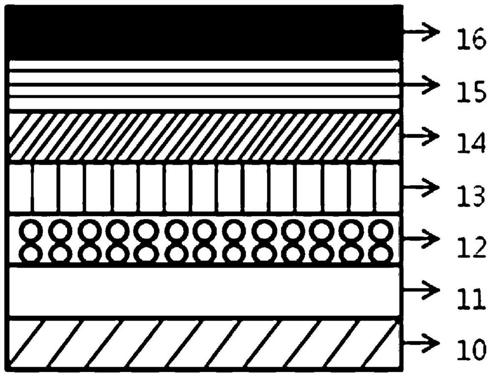
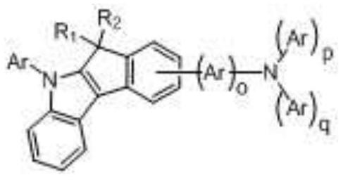
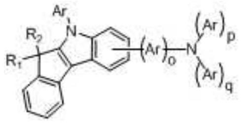
[0246] will be Thin film coated glass substrates with indium tin oxide (ITO) were cleaned ultrasonically with distilled water. After cleaning with distilled water, ultrasonically clean and dry with solvents such as isopropanol, acetone, methanol, etc., and then transfer to a plasma cleaner, use oxygen plasma to clean the above-mentioned substrate for 5 minutes, and then use a thermal vacuum coating machine (thermalevaporator) , on the top of the ITO substrate, the hole injection layer HT01 is fabricated film, compound 1 as a hole transport layer membrane. Then, as the above-mentioned light emitting layer, doped with BH01:BD01 5% to manufacture membrane. Then, as an electron transport layer, it was fabricated with Alq3:Liq (1:1) After the membrane, manufacture Liq film, Aluminum (Al) film, the device was sealed in a glove box (Encapsulation), thereby producing an organic light-emitting device.
Embodiment 2 to Embodiment 27
[0248] By the same method as in Example 1, an organic light-emitting device in which a hole injection layer and a hole transport layer were produced using Compounds 2 to 27, respectively, was produced.
Embodiment 28
[0250] will be Thin film coated glass substrates with indium tin oxide (ITO) were cleaned ultrasonically with distilled water. After cleaning with distilled water, ultrasonically clean and dry with solvents such as isopropanol, acetone, methanol, etc., and then transfer to a plasma cleaner, use oxygen plasma to clean the above-mentioned substrate for 5 minutes, and then use a thermal vacuum coating machine (thermalevaporator) , on the top of the ITO substrate, the hole injection layer HT01 is fabricated film, compound 1 as the first hole transport layer film and compound 25 as the second hole transport layer membrane. Then, as the above-mentioned light emitting layer, doped with BH01:BD01 5% to manufacture membrane. Then, as an electron transport layer, it was fabricated with Alq3:Liq (1:1) After the membrane, manufacture Liq Film, Aluminum (Al) film, the device was sealed in a glove box (Encapsulation), thereby producing an organic light-emitting device.
PUM
 Abstract
Description
Claims
Application Information
 - R&D
- Intellectual Property
- Life Sciences
- Materials
- Tech Scout
- Unparalleled Data Quality
- Higher Quality Content
- 60% Fewer Hallucinations
Browse by: Latest US Patents, China's latest patents, Technical Efficacy Thesaurus, Application Domain, Technology Topic, Popular Technical Reports.
© 2025 PatSnap. All rights reserved.Legal|Privacy policy|Modern Slavery Act Transparency Statement|Sitemap|About US| Contact US: help@patsnap.com


