Semiconductor device
一种半导体、鳞状的技术,应用在半导体器件、半导体/固态器件制造、半导体/固态器件零部件等方向,能够解决模塑树脂剥离等问题,达到密接力提高、小型化生产性和可靠性的效果
- Summary
- Abstract
- Description
- Claims
- Application Information
AI Technical Summary
Problems solved by technology
Method used
Image

Examples
Embodiment approach 1
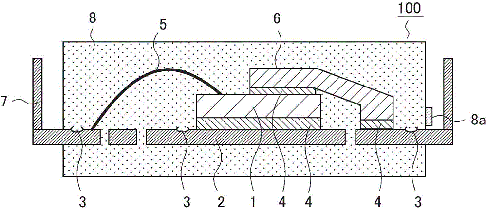
[0040] Next, the semiconductor device according to Embodiment 1 of the present invention will be described based on the drawings. figure 1 An example of the structure of the resin-molded semiconductor device according to Embodiment 1 is shown. The semiconductor device 100 according to Embodiment 1 is configured to include a semiconductor element 1 , a lead frame 2 , wires 5 , inner leads 6 , external terminals 7 , and the like. In addition, in all the following drawings, the same reference numerals are assigned to the same or corresponding parts in the drawings.
[0041] The semiconductor element 1 is, for example, an IGBT, MOSFET, IC chip, LSI chip, or the like, and is mounted on the upper surface of the lead frame 2 via a bonding member 4 such as solder or silver. The lead frame 2 on which the semiconductor element 1 or other electronic components are mounted is composed of a copper plate or a copper alloy plate, and its surface is coated with metal plating (not shown) suc...
Embodiment approach 2
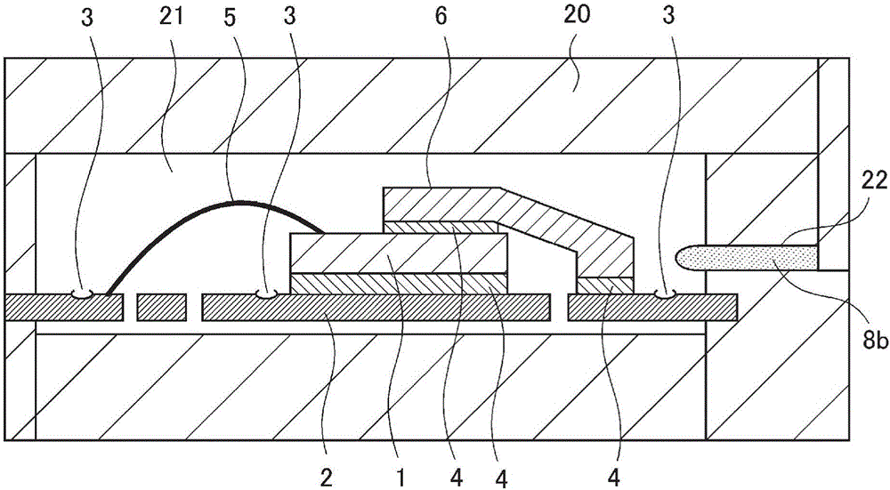
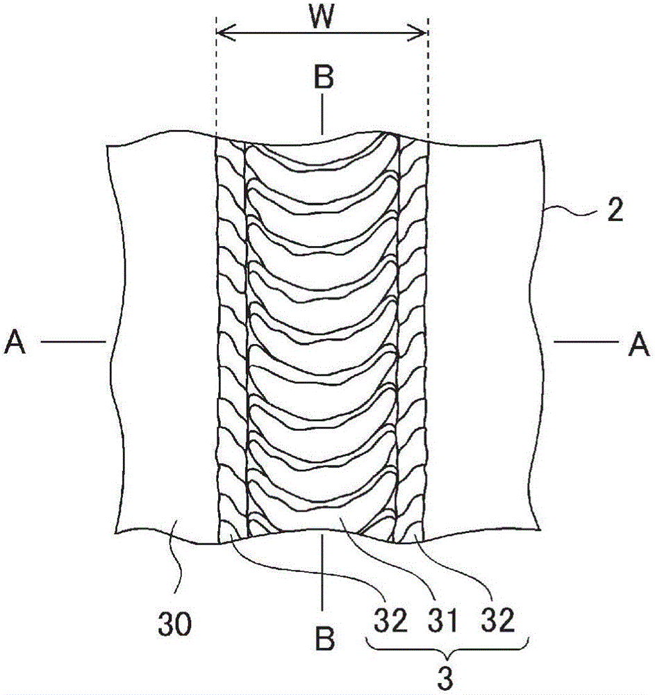
[0072] The overall structure of the semiconductor device according to the second embodiment of the present invention is the same as that of the above-mentioned first embodiment. figure 1 , and omit the description of each part. Figure 15 is a plan view showing the scale portion 3a of the semiconductor device 100 according to Embodiment 2, Figure 16 is in Figure 15 Sectional view obtained after section C-C is shown.
[0073] The scale portion 3 a of the second embodiment has an exposed portion 2 c where the lead frame 2 under the metal plating layer 30 , that is, copper or a copper alloy is exposed, near the center portion with a predetermined width W. The other structures are the same as those of the scale portion 3 in the first embodiment described above. Compared with the metal plating layer 30 , the exposed copper or copper alloy has higher adhesion to the molding resin 8 , and therefore, compared with the first embodiment described above, the peeling of the molding ...
Embodiment approach 3
[0078] In Embodiment 3 of the present invention, an example in which the scale portion 3 is applied to a semiconductor device having a structure different from that of the semiconductor device 100 in Embodiment 1 will be described. Figure 17 A semiconductor device 101 according to Embodiment 3 is shown. The semiconductor device 101 includes an electronic component 10 bridge-mounted so as to straddle between two separated regions of the lead frame 2 . The electronic component 10 is a capacitor, a thermistor, or the like.
[0079]In Embodiment 3, the two regions of the lead frame 2 on which the electronic component 10 is bridge-mounted may be a region where the semiconductor element 1 is mounted and a region where the semiconductor element 1 is not mounted, two regions where the semiconductor element 1 is mounted, and a region where the semiconductor element 1 is not mounted. Either of the two regions of the semiconductor element 1 .
[0080] When the electronic component 10 ...
PUM
 Abstract
Description
Claims
Application Information
 - Generate Ideas
- Intellectual Property
- Life Sciences
- Materials
- Tech Scout
- Unparalleled Data Quality
- Higher Quality Content
- 60% Fewer Hallucinations
Browse by: Latest US Patents, China's latest patents, Technical Efficacy Thesaurus, Application Domain, Technology Topic, Popular Technical Reports.
© 2025 PatSnap. All rights reserved.Legal|Privacy policy|Modern Slavery Act Transparency Statement|Sitemap|About US| Contact US: help@patsnap.com