Thin Film Transistor Substrate and Display Using the Same

一种薄膜晶体管、基板的技术,应用在电固体器件、半导体器件、电气元件等方向,能够解决低功耗有限等问题,达到低功耗属性的效果

Active Publication Date: 2017-03-08
LG DISPLAY CO LTD
View PDF3 Cites 9 Cited by
  • Summary
  • Abstract
  • Description
  • Claims
  • Application Information

AI Technical Summary

Problems solved by technology

However, there is a limit to achieving low power consumption using technologies associated with display devices developed so far

Method used


Image

  • Thin Film Transistor Substrate and Display Using the Same
  • Thin Film Transistor Substrate and Display Using the Same
  • Thin Film Transistor Substrate and Display Using the Same

Examples


no. 1 approach

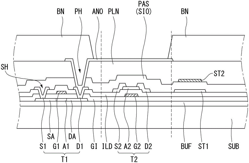
[0031] Reference figure 1 , We will explain the first embodiment of the present disclosure. figure 1 It is a cross-sectional view illustrating the structure of a thin film transistor substrate formed with two different types of thin film transistors for a flat panel display according to the first embodiment of the present disclosure. Here, we will mainly use cross-sectional views for explanation, because, for convenience, the cross-sectional views clearly show the main features of the present disclosure, and plan views are not used.

[0032] Reference figure 1 The thin film transistor substrate for a flat panel display according to the first embodiment includes a first thin film transistor T1 and a second thin film transistor T2 provided on the same substrate SUB. The first thin film transistor T1 and the second thin film transistor T2 may be disposed separately from each other, or they may be disposed within a relatively close distance. Otherwise, the two thin film transistors a...

no. 2 approach

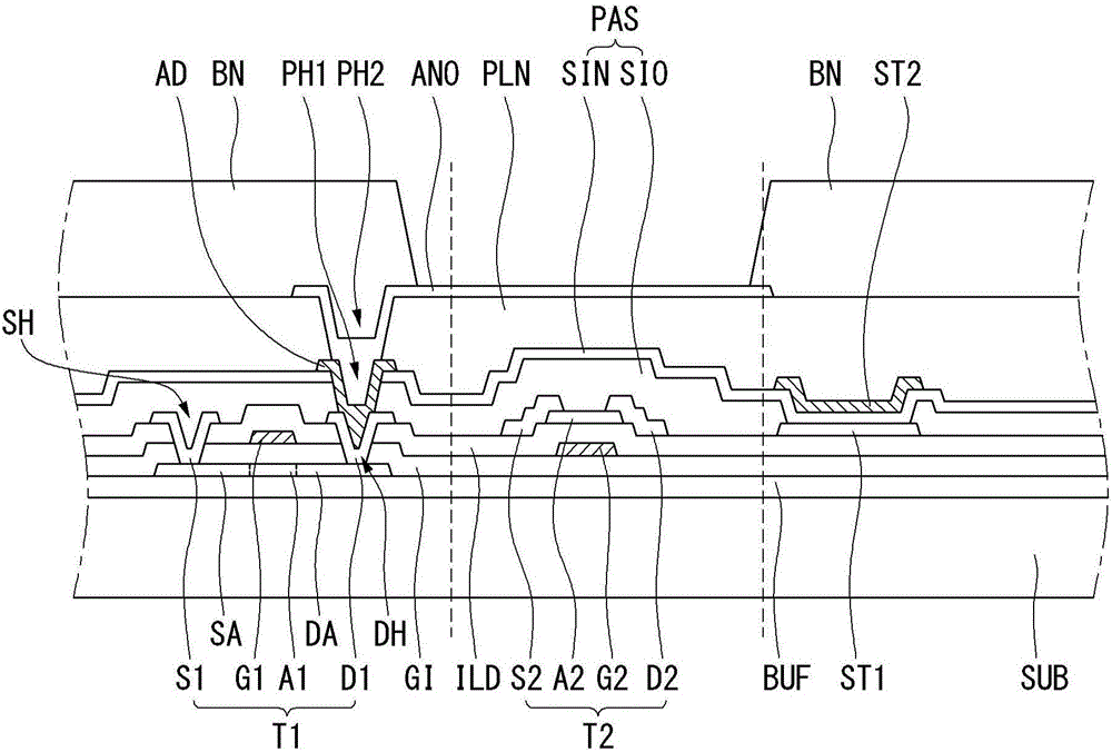
[0068] In the following, refer to image 3 , We will describe the second embodiment of the present disclosure. image 3 It is a cross-sectional view illustrating the structure of a thin film transistor substrate formed with two different types of thin film transistors for a flat panel display according to the second embodiment of the present disclosure.

[0069] In the first embodiment, in order to form a storage capacitor, the first storage capacitor electrode ST1 and the second storage capacitor electrode ST2 overlap the passivation layer PAS including the oxide layer SIO therebetween. In order to ensure surface properties and uniformity, the oxide layer SIO should have at least thickness of. Therefore, the interposed between the first storage capacitor electrode ST1 and the second storage capacitor electrode ST2 has at least The thickness of the oxide layer SIO forms a storage capacitor.

[0070] The oxide layer SIO has a lower dielectric constant (or permittivity) than the ni...


PUM


Abstract

The invention provides a thin film transistor substrate and display using the same. The display is disclosed which includes a substrate, a first thin film transistor, a second thin film transistor, a first storage capacitor electrode, an oxide layer, a nitride layer, a second storage capacitor electrode, a planar layer and a pixel electrode. The first thin film transistor is disposed in a first area on the substrate. The second thin film transistor is disposed in a second area on the substrate. The first storage capacitor electrode is disposed in a third area on the substrate. The oxide layer covers the first thin film transistor and the second thin film transistor, and exposes the first storage capacitor electrode. The nitride layer is disposed on the oxide layer and covers the first storage capacitor electrode. The second storage capacitor electrode includes a first metal layer and a second metal layer, and overlaps with the first storage capacitor electrode on the nitride layer. The planar layer covers the first thin film transistor, the second thin film transistor and the second storage capacitor electrode. The pixel electrode is disposed on the planar layer.

Description

Technical field [0001] The present disclosure relates to a thin film transistor substrate having two different types of thin film transistors on the same substrate and a display using the thin film transistor substrate. Background technique [0002] Nowadays, with the development of the information society, the requirements for displays for presenting information are getting higher and higher. Therefore, various flat panel displays (or "FPD") have been developed to overcome many of the disadvantages of the heavy and bulky cathode ray tube (or "CRT"). Flat panel display devices include liquid crystal display devices (or “LCD”), plasma display panels (or “PDP”), organic light emitting display devices (or “OLED”), and electrophoretic display devices (or “ED”). [0003] The display panel of the flat panel display may include a thin film transistor substrate having thin film transistors distributed in respective pixel regions arranged in a matrix. For example, a liquid crystal display...

Claims


Application Information

Patent Timeline
Patent Type & Authority Applications(China)
IPC IPC(8): H01L27/12
CPCH01L27/1251H01L27/1255H01L27/1259H01L27/1225
Inventor 卢韶颖
Owner LG DISPLAY CO LTD
Why Eureka
Try Eureka