
A method for etching silicon dioxide

A technology of silicon dioxide and etching time, applied in the direction of instruments, light guides, optics, etc., can solve the problems of hindering etching reaction, large difference, slow etching rate, etc., to reduce the etching load effect and reduce the depth poor, performance-improving effect

Active Publication Date: 2020-01-03
BEIJING NAURA MICROELECTRONICS EQUIP CO LTD
View PDF6 Cites 0 Cited by
  • Summary
  • Abstract
  • Description
  • Claims
  • Application Information

AI Technical Summary

Problems solved by technology

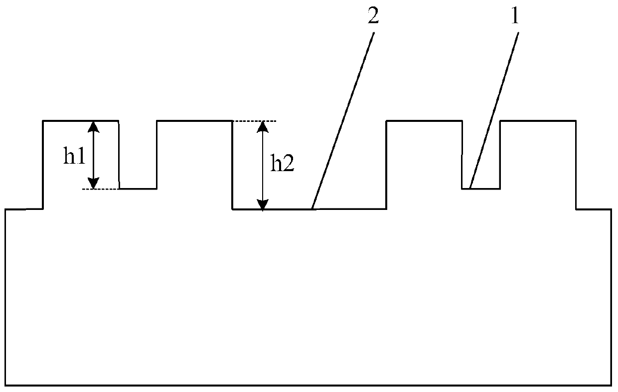
[0004] The inventors of the present application have found that during the etching process, the polymer produced by the chemical reaction of octafluorocyclobutane is deposited on the bottom of the narrow groove 1, and as the etching depth increases, the plasma formed by argon gas The bombardment cannot completely remove the polymer deposited at the bottom of the narrow groove 1, resulting in an increase in the deposited polymer, which eventually hinders the etching reaction, making the etching rate of the narrow groove 1 slower, and the depth h1 of the narrow groove 1 is relatively small. As a result, the difference between the depth h1 of the narrow groove 1 and the depth h2 of the wide groove 2 is relatively large, resulting in an obvious etching load effect of silicon dioxide, which affects the performance of the silicon dioxide optical waveguide device

Method used


Image

  • A method for etching silicon dioxide
  • A method for etching silicon dioxide
  • A method for etching silicon dioxide

Examples


Embodiment Construction

[0032] The following will clearly and completely describe the technical solutions in the embodiments of the present invention with reference to the accompanying drawings in the embodiments of the present invention. Obviously, the described embodiments are only some, not all, embodiments of the present invention. Based on the embodiments of the present invention, all other embodiments obtained by persons of ordinary skill in the art without creative efforts fall within the protection scope of the present invention.

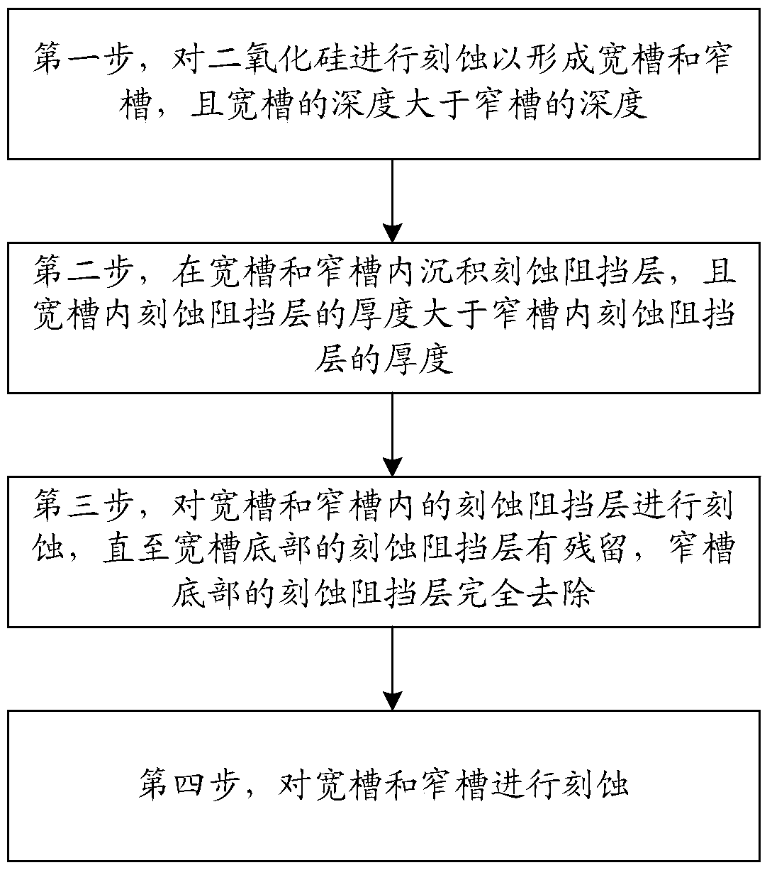
[0033] The embodiment of the present invention provides a silicon dioxide etching method, such as figure 2 As shown, the etching method includes:

[0034] In the first step, silicon dioxide is etched to form wide grooves and narrow grooves, and the depth of the wide grooves is greater than that of the narrow grooves.

[0035] In the process of etching silicon dioxide, the etching gas easily enters the wide groove, and the reaction by-products in the wide groove a...


PUM

PropertyMeasurementUnit
widthaaaaaaaaaa

Abstract

The invention discloses an etching method of silica, and relates to the etching technology field. By adopting the etching method, the etching load effect of the silica is relieved. The etching method comprises steps that step 1, the silica is etched to form a wide groove and a narrow groove, and the depth of the wide groove is greater than the depth of the narrow groove; step 2, etching barrier layers are deposited respectively in the wide groove and the narrow groove, and the thickness of the etching barrier layer in the wide groove is greater than the thickness of the etching barrier layer in the narrow groove; step 3, the etching of the etching barrier layer in the wide groove and the etching of the etching barrier layer in the narrow groove are carried out, until the residues of the etching barrier layer of the bottom part of the wide groove exist, and the etching barrier layer of the bottom part of the narrow groove is totally removed; step 4, the wide groove and the narrow groove are etched. The etching method is used for etching a silica optical waveguide.

Description

technical field [0001] The invention relates to the technical field of etching, in particular to a silicon dioxide etching method. Background technique [0002] In the field of optics, the optical waveguide technology that fabricates several optical passive devices on the same substrate and interconnects them to form functional circuits through waveguides is a very practical technology. Because silica optical waveguides have good optical, electrical, mechanical properties and thermal stability, and are low in cost, silica optical waveguides are widely used in the field of optical waveguide technology. [0003] figure 1 It is a partial cross-sectional schematic diagram of a silicon dioxide optical waveguide in the prior art, and the silicon dioxide optical waveguide has a narrow groove 1 and a wide groove 2 . Silicon dioxide is usually etched by a dry etching method to form a silicon dioxide optical waveguide with the above structure, for example, silicon dioxide is etched ...

Claims


Application Information

Patent Timeline
Patent Type & Authority Patents(China)
IPC IPC(8): G02B6/136G02B6/132
CPCG02B6/132G02B6/136
Inventor 谢秋实
Owner BEIJING NAURA MICROELECTRONICS EQUIP CO LTD
Learn More