PCB photoelectric image obtaining and pre-treating method

A preprocessing and image technology, applied in image data processing, image enhancement, image analysis, etc., can solve the problems of unsuitable contrast, low PCB photoelectric image, etc., and achieve the effect of clear and visible image details

Inactive Publication Date: 2017-03-22
HUNAN UNIV OF ARTS & SCI
View PDF0 Cites 5 Cited by
  • Summary
  • Abstract
  • Description
  • Claims
  • Application Information

AI Technical Summary

Problems solved by technology

However, these algorithms are not suitable for PCB photoelectric images with low contrast after splicing

Method used


Image

  • PCB photoelectric image obtaining and pre-treating method
  • PCB photoelectric image obtaining and pre-treating method
  • PCB photoelectric image obtaining and pre-treating method

Examples


Embodiment Construction

[0017] Below in conjunction with accompanying drawing and embodiment the present invention is further described:

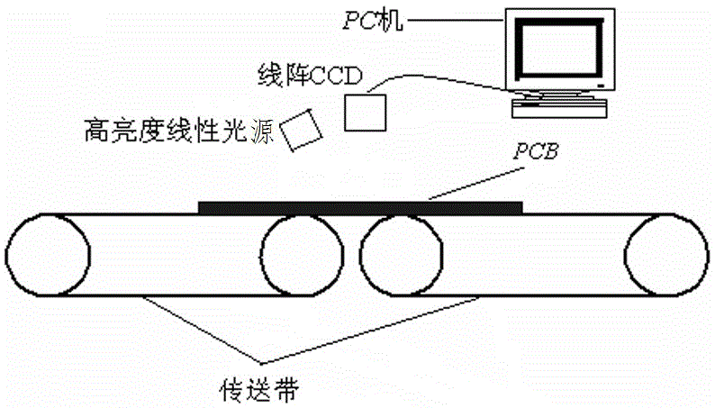
[0018] The method of acquisition and preprocessing of the designed PCB photoelectric image, such as figure 1 Shown: First, the conveyor belt is driven by a high-precision stepper / servo motor system to rotate at a uniform speed; then the PCB is driven by the conveyor belt to perform a high-precision uniform-speed linear motion due to friction; then several CCDs are formed. One-dimensional linear array CCD, distributed along the width direction of the PCB; fix the high-brightness linear light source above the PCB along the width direction of the PCB, and illuminate the local PCB directly below the CCD; then the partial PCB photoelectric image captured by the linear array CCD is passed through the PC The image acquisition card in the machine collects, and the Visual C++ program adopts the automatic stitching algorithm to complete the image stitching work. With the un...


PUM


Abstract

A PCB photoelectric image obtaining and pre-treating method including the steps of allowing a conveyor belt to rotate at a uniform speed when driven by a high-precision step servo motor system, the conveyor belt driving a PCB to conduct high-precision uniform-speed linear motion under the friction force effect, distributing a one-dimensional linear array CCD formed by a plurality of CCDs along the width direction of the PCB, fixing a high brightness linear light source above the PCB along the width direction to irradiate partial PCB right below the CCD, and an image acquisition card in a PC acquiring partial PCB photoelectric images taken by the linear array CCD to obtain a PCB photoelectric image of a complete area. Since an algorithm combing removing gray redundance (RGR) and gray transformation (GT) is employed, the non-redundant gray level of an image is maintained, and the details of the image are clear and distinct. The method is suitable for companies producing or researching large area printed circuit boards (PCB).

Description

technical field [0001] The invention relates to a method for acquiring and preprocessing a photoelectric image, in particular to a method for acquiring and preprocessing a photoelectric image of a PCB. Background technique [0002] In the printed circuit board (Printed Circuit Board, referred to as PCB) detection and identification system, the acquisition and preprocessing of PCB photoelectric images are very important. In the acquisition system of large-area PCB photoelectric images, due to the limitation of the field of view of the CCD lens, the linear array CCD is only used to capture partial images along a certain direction of the PCB, so the partial images must be stitched to obtain a complete PCB photoelectric image. image; and the spliced ​​PCB photoelectric image contains noise, overall dark and low contrast due to the external conditions in the acquisition process and the splicing algorithm itself, which brings difficulties to follow-up work such as image recognitio...

Claims


Application Information

Patent Timeline
IPC IPC(8): G06T3/40G06T5/00G06T5/20G06T5/40G06T7/136
CPCG06T3/4038G06T5/20G06T5/40G06T7/0004G06T2207/30141G06T2207/10004G06T2207/20004G06T2207/20032G06T5/90G06T5/70
Inventor 乔闹生
Owner HUNAN UNIV OF ARTS & SCI
Why Eureka
Try Eureka