
A chip input pin testing method and device

A test device and test method technology, applied in the direction of measuring device, single semiconductor device test, semiconductor/solid-state device test/measurement, etc., can solve problems such as waste of material and financial resources, high test cost, and complicated chip replacement

Active Publication Date: 2019-04-16
FUZHOU ROCKCHIP SEMICON
View PDF4 Cites 0 Cited by
  • Summary
  • Abstract
  • Description
  • Claims
  • Application Information

AI Technical Summary

Problems solved by technology

[0003] For this reason, need to provide a kind of technical scheme of chip input pin test, in order to solve existing chip pin test method, can only test the function of chip pin again on the complete machine after chip installation, cause Problems such as high test cost, complicated chip replacement, waste of a lot of material and financial resources, etc.

Method used


Image

  • A chip input pin testing method and device
  • A chip input pin testing method and device
  • A chip input pin testing method and device

Examples


Embodiment Construction

[0042] In order to explain in detail the technical content, structural features, achieved goals and effects of the technical solution, the following will be described in detail in conjunction with specific embodiments and accompanying drawings.

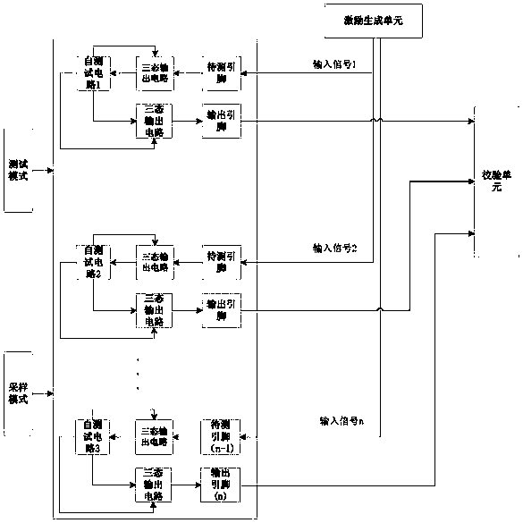
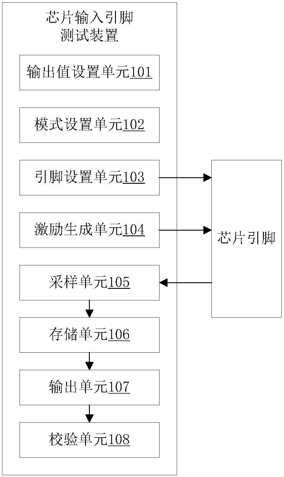
[0043] see figure 1 , a schematic diagram of a chip input pin testing device according to an embodiment of the present invention.

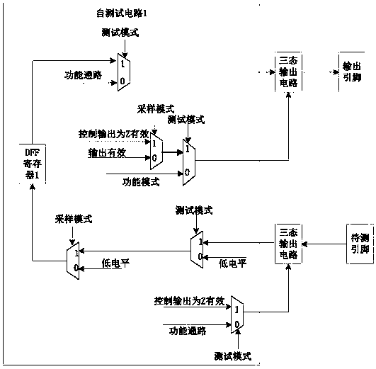
[0044] The chip includes at least one pin to be tested, and the device includes an output value setting unit 101, a mode setting unit 102, a pin setting unit 103, an excitation generating unit 104, a sampling unit 105, a storage unit 106, an output unit 107 and a calibration unit. Test unit 108. Pins, also known as pins, are the wiring from the internal circuit of the integrated circuit (chip) to the peripheral circuit, and all the pins constitute the external interface of the chip.

[0045] The output value setting unit 101 is used to set an output preset value;

[0046] The mode setting unit 102 is u...


PUM


Abstract

The invention provides a chip input pin test method and device. The method switches the current mode of a chip according to a control signal, inputs an excitation sequence to the to-be-tested pin of the chip, and then stores a value received by the to-be-tested pin in a storage unit by using a sampling unit, outputs the value of the storage unit by an output pin (another pin with a good output function and corresponding to the to-be-tested pin) corresponding to the to-be-tested pin, compares the output value with a preset output value mirror at a verifying unit so as to automatically check whether the input function of the to-be-tested pin of the chip is normal. Thus, testing can be carried out in a bare chip stage, which is equivalent to a whole test method, thereby greatly reducing test cost. In addition, the input excitation sequence can be customized according to actual needs, and has high flexibility and fault detection coverage.

Description

technical field [0001] The invention relates to the field of chip testing, in particular to a chip input pin testing method and device. Background technique [0002] In the current chip testing technology, it is impossible to conveniently test the pins of the chip. It is usually necessary to wait until the chip is packaged, and then configure the relevant sequence when the whole machine software is running to fully test the pin function of the chip. With the rapid development of chip feature process size, chip pins are more and more prone to yield problems, so the test of chip pins has become a very important part in the field of chip testing. If the pin test fails, the chip will not be able to input or output data accurately, which will directly affect the performance of the chip. If the existing test method is still used, the chip pins can only be verified when the whole machine is verified. If the pins fail, because the time to find the problem is too late, the chip has...

Claims


Application Information

Patent Timeline
IPC IPC(8): H01L21/66G01R31/26
CPCG01R31/2601H01L22/14H01L22/34
Inventor 林源晟
Owner FUZHOU ROCKCHIP SEMICON
Features
  • Generate Ideas
  • Intellectual Property
  • Life Sciences
  • Materials
  • Tech Scout
  • Unparalleled Data Quality
  • Higher Quality Content
  • 60% Fewer Hallucinations
Learn More