Array substrate, display panel and preparation method of array substrate

An array substrate and substrate technology, which is applied in semiconductor/solid-state device manufacturing, semiconductor devices, electrical components, etc., can solve problems such as undercutting and chamfering at the bottom of via holes, so as to ensure electrical connection performance, improve product yield and display effect Effect

Active Publication Date: 2017-03-22
HEFEI BOE OPTOELECTRONICS TECH +1
View PDF3 Cites 0 Cited by
  • Summary
  • Abstract
  • Description
  • Claims
  • Application Information

AI Technical Summary

Problems solved by technology

[0005] The present invention aims at the above-mentioned deficiencies in the prior art, and provides an array substrate, a display panel, and a preparation method for the array substrate, which are used to at least partially solve the problem of undercutting and chamfering at the bottom of the via hole during the via hole process of the insulating layer

Method used


Image

  • Array substrate, display panel and preparation method of array substrate
  • Array substrate, display panel and preparation method of array substrate
  • Array substrate, display panel and preparation method of array substrate

Examples


Embodiment Construction

[0040] The technical solutions in the present invention will be clearly and completely described below in conjunction with the accompanying drawings in the present invention. Apparently, the described embodiments are part of the embodiments of the present invention, not all of them. Based on the embodiments of the present invention, all other embodiments obtained by persons of ordinary skill in the art without making creative efforts belong to the protection scope of the present invention.

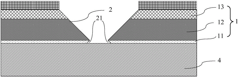
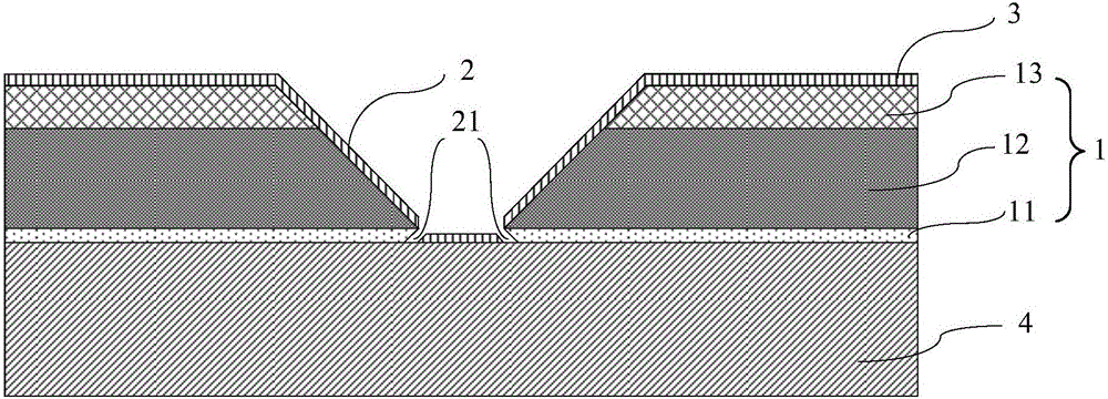
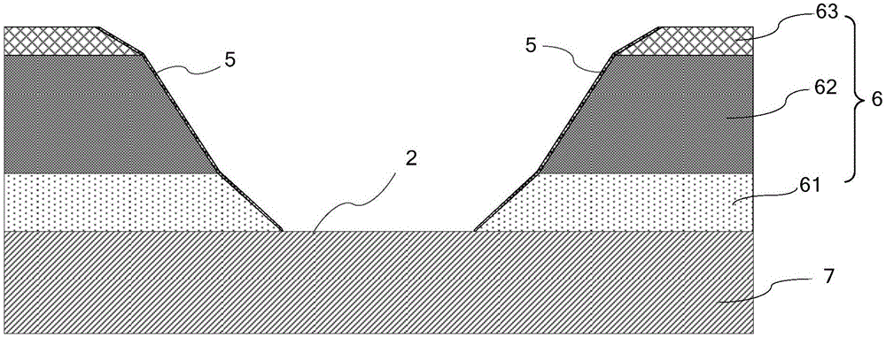
[0041] The following combination figure 2 , detailing the structure of the array substrate of the present invention.

[0042] Such as figure 2 As shown, the present invention provides an array substrate, including a substrate (not shown in the figure), a first insulating layer 61, a second insulating layer 62, a third insulating layer 63, and and the via hole 2 of the third insulating layer 63 . The first insulating layer 61, the second insulating layer 62 and the third insulating lay...


PUM


Abstract

The invention provides an array substrate, a display panel and a preparation method of the array substrate. A protective film layer is formed at the position, at least corresponding to a first insulating layer, on the side wall of a via hole which penetrates through the first insulating layer, a second insulating layer and a third insulating layer, and an undercut chamfer at the bottom of the via hole can be avoided, so that the electric connection property between two layer structures connected through the via hole is ensured, and the yield and the display effects of the array substrate and the display panel are improved.

Description

technical field [0001] The invention relates to the field of display technology, in particular to an array substrate, a display panel and a method for preparing the array substrate. Background technique [0002] In the preparation process of the array substrate, after the top passivation protective layer is fabricated, it is necessary to use dry etching technology to form via holes on the passivation layer, and then form ITO (Indium Tin Oxide, Indium Tin Oxide) on the surface of the passivation layer. ) layer, so that the ITO layer is electrically connected to the source-drain electrode layer. [0003] combine Figure 1a with Figure 1b As shown, in the traditional array substrate preparation process, the material of the passivation layer 1 is usually SiNx, and the passivation layer 1 is divided into three layers, including the passivation transition layer 11, the passivation body layer 12 and the passivation top layer 13, The function of the passivation transition layer 1...

Claims


Application Information

Patent Timeline
Patent Type & Authority Applications(China)
IPC IPC(8): H01L27/12H01L27/15H01L21/768H01L21/3065
CPCH01L27/1203H01L27/1259H01L27/15H01L21/3065H01L21/76802
Inventor 宫奎
Owner HEFEI BOE OPTOELECTRONICS TECH
Why Eureka
Try Eureka