
Anisotropic conductive adhesive film and peeling method of anisotropic conductive adhesive film

A technology of anisotropic conductive adhesive and conductive particles, which is applied in the direction of circuits, electrical components, electric solid devices, etc., can solve the problem that the anisotropic conductive adhesive film is difficult to scrape off, the lines on the substrate are easy to scrape, and it cannot be re-glued by rework Solve problems such as COF chips, achieve the effect of easy scraping and cleaning, little damage to raw materials, and improve the success rate of rework

Active Publication Date: 2018-07-20
WUHAN CHINA STAR OPTOELECTRONICS TECH CO LTD
View PDF4 Cites 0 Cited by
  • Summary
  • Abstract
  • Description
  • Claims
  • Application Information

AI Technical Summary

Problems solved by technology

[0004] The technical problem to be solved by the present invention is to provide a kind of stripping method of anisotropic conductive adhesive film and anisotropic conductive adhesive film, in order to solve the problem that the anisotropic conductive adhesive film is difficult to scrape off in the prior art, if a squeegee stick is used Scratching hard, it is easy to scrape the lines on the substrate, and it cannot be used for rework and rebonding of COF chips

Method used


Image

  • Anisotropic conductive adhesive film and peeling method of anisotropic conductive adhesive film
  • Anisotropic conductive adhesive film and peeling method of anisotropic conductive adhesive film
  • Anisotropic conductive adhesive film and peeling method of anisotropic conductive adhesive film

Examples


Embodiment Construction

[0027] The following will clearly and completely describe the technical solutions in the embodiments of the present invention with reference to the accompanying drawings in the embodiments of the present invention. Obviously, the described embodiments are only some, not all, embodiments of the present invention. Based on the embodiments of the present invention, all other embodiments obtained by persons of ordinary skill in the art without making creative efforts belong to the protection scope of the present invention.

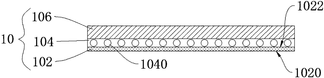
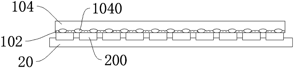
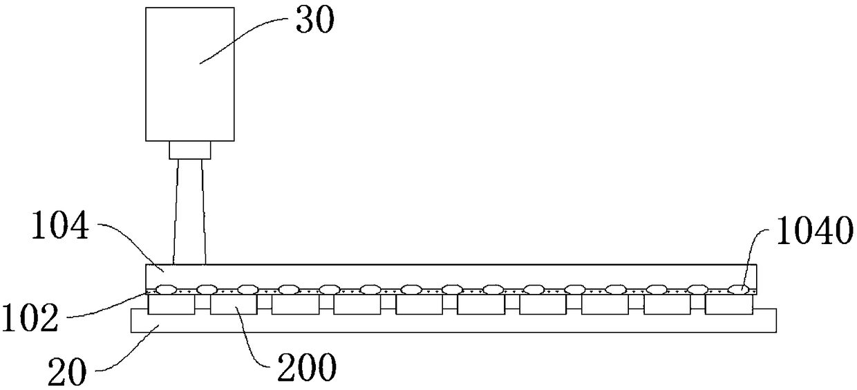
[0028] Please also refer to figure 1 and figure 2 The anisotropic conductive adhesive film 10 is used to connect the driver chip and the substrate 20. The anisotropic conductive adhesive film 10 includes a connected buffer layer 102 and an anisotropic conductive adhesive layer 104. The buffer layer 102 is directly pasted on the substrate 20. The directional conductive adhesive layer 104 is located on the side of the buffer layer 102 away from the substrate 2...


PUM


Abstract

The invention discloses an anisotropic conductive adhesive film. The anisotropic conductive adhesive film includes a stacked buffer layer and an anisotropic conductive adhesive layer. The buffer layer includes a first surface and a second surface oppositely arranged. , the first surface is used to be directly pasted on the substrate, the second surface is pasted on the anisotropic conductive adhesive layer and completely covers the anisotropic conductive adhesive layer on the second surface Orthographic projection, the buffer layer includes hydrogenated silicon, which is used to generate bubbles to separate the anisotropic conductive adhesive layer from the substrate after being irradiated by laser light, and the anisotropic conductive adhesive layer includes conductive particles for conduction The driving chip and the substrate. The invention also discloses a stripping method of the anisotropic conductive adhesive film. The anisotropic conductive adhesive film is irradiated with laser light to decompose the silicon hydride in the buffer layer to generate hydrogen bubbles to separate the anisotropic conductive adhesive layer and the substrate, so that the anisotropic conductive adhesive film is easy to scrape clean and improve the success rate of rework of defective products.

Description

technical field [0001] The invention relates to the field of display technology, in particular to an anisotropic conductive adhesive film and a peeling method of the anisotropic conductive adhesive film. Background technique [0002] With continuous advancement of display technology, active-matrix organic light emitting diode (AMOLED) displays are more and more widely used. The AMOLED display mainly uses Anisotropic Conductive Film (ACF) to bond Chip On Flex / Chip OnFilm (COF) driver chips on the substrate of the display panel. Due to the low yield rate of the existing COF bonding process, there are more and more cases of rework and rework of defective products. Due to the high cost of COF chips and display panels, it is particularly important to improve the quality of rework. How to design an anisotropic conductive adhesive film that is easy to peel off in the rework process, and how to peel off the cured and bonded anisotropic conductive adhesive film on the substrate with...

Claims


Application Information

Patent Timeline
Patent Type & Authority Patents(China)
IPC IPC(8): H01L51/52H01L51/56
CPCH10K50/80H10K71/00
Inventor 黄添旺崔磊
Owner WUHAN CHINA STAR OPTOELECTRONICS TECH CO LTD
Learn More