Printed circuit board with porous structure resistance layer, and manufacturing method for printed circuit board
A technology of printed circuit board and manufacturing method, which is applied in the directions of printed circuit manufacturing, printed circuit, removal of conductive materials by chemical/electrolytic methods, etc., can solve problems such as poor thermal stability of resistance layer, and achieve good thermal stability and square resistance. Large, productive effects
- Summary
- Abstract
- Description
- Claims
- Application Information
AI Technical Summary
Problems solved by technology
Method used
Image

Examples
Embodiment 1
[0027] The method for manufacturing a printed circuit board with a porous structure resistance layer includes the following steps: 1. According to the required pattern, paste the first photoresist layer on the conductor layer on the printed circuit board, and perform the first exposure, The first development, the first etching, and the first photoresist; the printed circuit board here is any one of rigid board, flexible board and rigid-flexible board; the insulating medium of the printed circuit board here is Any one of epoxy resin, polytetrafluoroethylene, phenolic resin, polyphenylene ether resin, BT resin, polyimide, liquid crystal polymer, polyester and hydrocarbon-ceramic blend, wherein, here The conductor layer is a copper foil layer, and the conductor layer is arranged inside or outside the printed circuit board.
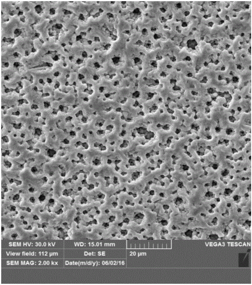
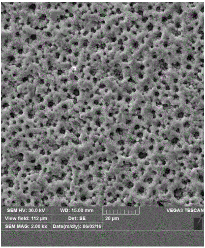
[0028] 2. Roughening and catalyst adsorption on the surface of the printed circuit board: use chemical methods and / or physical methods to increase the roughn...
Embodiment 2
[0047] 1. After the copper-clad substrate is cleaned and micro-etched with 3% sulfuric acid, hydrogen peroxide-sulfuric acid, a layer of dry film is pressed on the surface, then exposed, developed with 5% sodium carbonate solution, etched with sodium chlorate-copper chloride solution, and finally After being treated with 5% sodium hydroxide solution, the dry film on the surface of the substrate is peeled off, leaving a pre-designed circuit pattern.
[0048] 2. After the action of alkaline potassium permanganate at 85°C, the surface of the circuit board is roughened, forming a microscopically rough and uneven shape.
[0049] 3. The circuit board is continuously subjected to the following treatments to deposit catalyst palladium on its surface:
[0050] Activation - the purpose is to adsorb the colloid composed of palladium and tin on the surface of the circuit board;
[0051] Acceleration - peel off the tin layer on the surface of the palladium colloid to expose the catalytic ...
PUM
| Property | Measurement | Unit |
|---|---|---|
| Thickness | aaaaa | aaaaa |
Abstract
Description
Claims
Application Information
 - R&D Engineer
- R&D Manager
- IP Professional
- Industry Leading Data Capabilities
- Powerful AI technology
- Patent DNA Extraction
Browse by: Latest US Patents, China's latest patents, Technical Efficacy Thesaurus, Application Domain, Technology Topic.
© 2024 PatSnap. All rights reserved.Legal|Privacy policy|Modern Slavery Act Transparency Statement|Sitemap