Method and apparatus for producing ultra-thin semiconductor chip and method and apparatus for producing ultra-thin back-illuminated solid-state image pickup device

a pickup device and semiconductor chip technology, applied in the direction of semiconductor/solid-state device details, radiation control devices, diodes, etc., can solve the problems of increasing the noise of fixed pattern noise due to dark current, the inability to use back-illuminated, and the uneven light reception sensitivity of the ccd sensor. achieve the effect of improving yield, quality and productivity, and improving separation performan

Inactive Publication Date: 2005-04-07
SONY CORP
View PDF3 Cites 156 Cited by
  • Summary
  • Abstract
  • Description
  • Claims
  • Application Information

AI Technical Summary

Benefits of technology

[0022] An object of the present invention is to provide a method and an apparatus for producing an ultra-thin semiconductor chip, more particularly an ultra-thin back-illuminated solid-state image pickup device, utilizing a single crystalline semiconductor layer formed on a single crystalline support substrate (hereinafter referred to as a “support substrate”) via an insulating layer and improving a separation performance of this single crystalline semiconductor layer from the support substrate so as to enable an improvement of the yield, quality, and productivity.
[0029] In the present invention, in order to produce an ultra-thin semiconductor chip, particularly an ultra-thin back-illuminated solid-state image pickup device, comprised of a first single crystalline semiconductor layer on which a semiconductor device unit, particularly a solid-state image pickup sensor unit, and projecting connection electrodes to be connected to the semiconductor device unit, particularly the solid-state image pickup sensor unit, are formed, the present invention uses a base comprised of a support substrate on which an ion implanted layer or porous substance peeling layer, second single crystalline semiconductor layer, insulating layer, and first single crystalline semiconductor layer are stacked and improves the peeling of the support substrate by adopting the following steps.
[0031] Then, it forms a resin protective film filling the interior of the score and covering the surface of the first single crystalline semiconductor layer so as to impart strain of curing shrinkage stress of the resin protective film to the peeling layer of the support substrate to thereby facilitate peeling of the support substrate using the peeling layer as an interface.
[0032] Further, it polishes one surface of the resin protective film to expose the projecting connection electrodes at the surface and covers the resin protective film surface and the projecting connection electrode surfaces by a conductive protective tape free from residual conductive adhesive, for example, a UV-ray curable tape, to prevent static electricity damage up to the time of peeling and the time of mounting on a mounting board.
[0035] According to a seventh aspect of the present invention, there is provided a production apparatus of an ultra-thin semiconductor chip, particularly a production apparatus of an ultra-thin back-illuminated solid-state image pickup device, discharging to a substrate having at least two porous semiconductor peeling layers inside it for example a liquid (water, an etching solution, alcohol, etc.), a gas (air, nitrogen, argon, etc.), a mixture of a liquid and a gas mixing the gas in the liquid in an appropriate ratio, or a fluid of the same containing ultra-fine particle powder of solid granules and powder (polishing agent, ice, pieces of plastic, etc.) from one or more fine nozzles to separate the substrate at a predetermined porous semiconductor peeling layer as an interface during rotation, which production apparatus of an ultra-thin semiconductor chip, particularly production apparatus of an ultra-thin back-illuminated solid-state image pickup device, has support portions for rotatably supporting front and backs of the substrate; a discharge portion for discharging the fluid toward a porous semiconductor peeling layer; and a stopper portion for preventing the fluid from the discharging portion from striking other porous semiconductor peeling layers.
[0036] According to the production apparatus of an ultra-thin semiconductor chip, particularly the production apparatus of an ultra-thin back-illuminated solid-state image pickup device, of the above present invention, since there is provided a stopper portion for preventing fluid from the discharging portion from striking the other porous semiconductor peeling layers when discharging fluid to a substrate having at least two porous semiconductor peeling layers inside it to separate the substrate using a predetermined porous semiconductor peeling layer as an interface, the peeling action by the fluid is prevented from acting upon the other porous semiconductor peeling layers and the substrate is separated using the intended porous semiconductor peeling layer as an interface.

Problems solved by technology

A usual silicon substrate has a thickness of 400 to 500 μm, however, so it cannot be used as is for a back-illuminated.
Summarizing the problems to be solved by the invention, with such mechanical, chemical, or mechanical and chemical methods, variation occurs in the substrate thickness needed at the center of the back of the chip where light etc. will strike, the light reception sensitivity of the CCD sensor will become uneven, fixed pattern noise due to dark current will increase, and other problems will easily arise.
Further, a chip becomes susceptible to mechanical shock and temperature changes along with the reduction of the thickness, so breaks, becomes chipped, etc. leading to a drop in the yield and the quality.
Also, the increase in the number of work steps leads to a deterioration of the productivity and consequently an unavoidable increase in costs.
The above method is characterized by separating the seed Si wafer at the porous Si layer by a water jet, but the thinner this single crystalline Si layer and the larger the wafer size, the harder the separation and the more easily problems arise in the yield and quality due to breakage, chipping, cracks, etc.
Further, the technology disclosed in Japanese Unexamined Patent Publication (Kokai) No. 11-195562 calls for forming a plurality of porous Si layers having different porosities as the above porous layer to thereby facilitate the peeling, but in this case as well, similarly, at the time of peeling by tension the porous Si layer, problems easily arise in the yield and quality due to breakage, chipping, cracks, etc.
In this method as well, the thinner this single crystalline Si layer and the larger the wafer size, the harder the separation and easier problems arise in the yield and quality due to breakage, chipping, cracks. etc.
As explained above, when trying to fabricate a thin semiconductor chip and a thin back-illuminated solid-state image pickup device by utilizing these well known SOI substrate fabrication processes, in each case, separation becomes difficult when the wafer size becomes large and consequently there is a problem in the yield, quality, and reliability due to breakage, chipping, cracks, etc.

Method used


Image

  • Method and apparatus for producing ultra-thin semiconductor chip and method and apparatus for producing ultra-thin back-illuminated solid-state image pickup device
  • Method and apparatus for producing ultra-thin semiconductor chip and method and apparatus for producing ultra-thin back-illuminated solid-state image pickup device
  • Method and apparatus for producing ultra-thin semiconductor chip and method and apparatus for producing ultra-thin back-illuminated solid-state image pickup device

Examples


first embodiment

[0066] First Embodiment

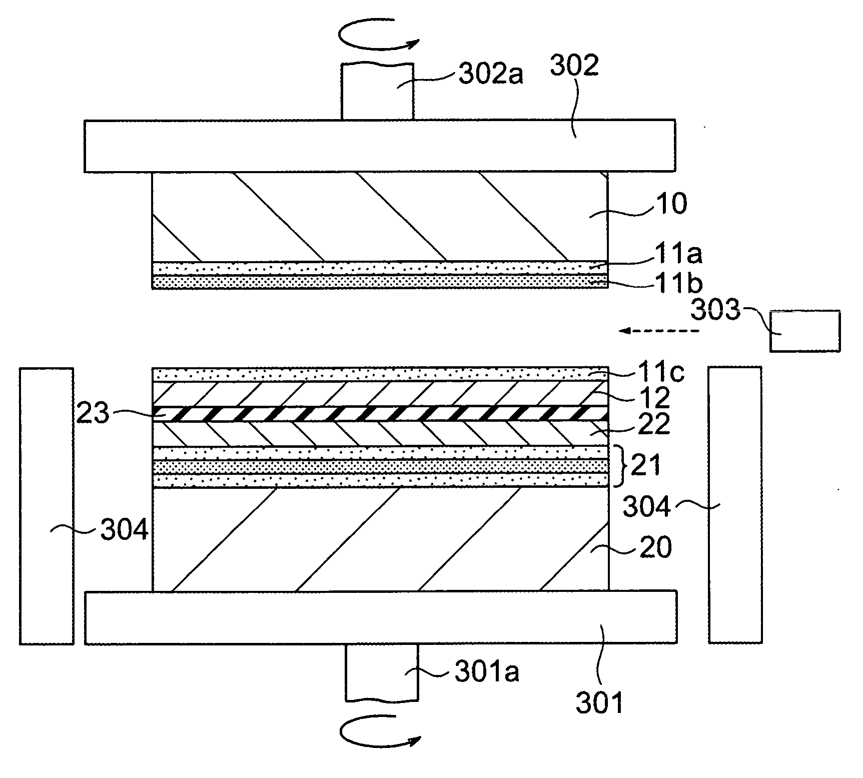
[0067] In the present embodiment, the explanation will be given of a method of production and production apparatus of a back-illuminated solid-state image pickup device of a single-surface resin sealed ultra-thin chip size hollow package using the double porous layer separation method (for example the method of separating a seed substrate by a first porous Si layer formed on a seed substrate and separating the support substrate by a second porous Si layer formed on the support substrate) among the methods of fabrication of new ultra-thin SOI substrates.

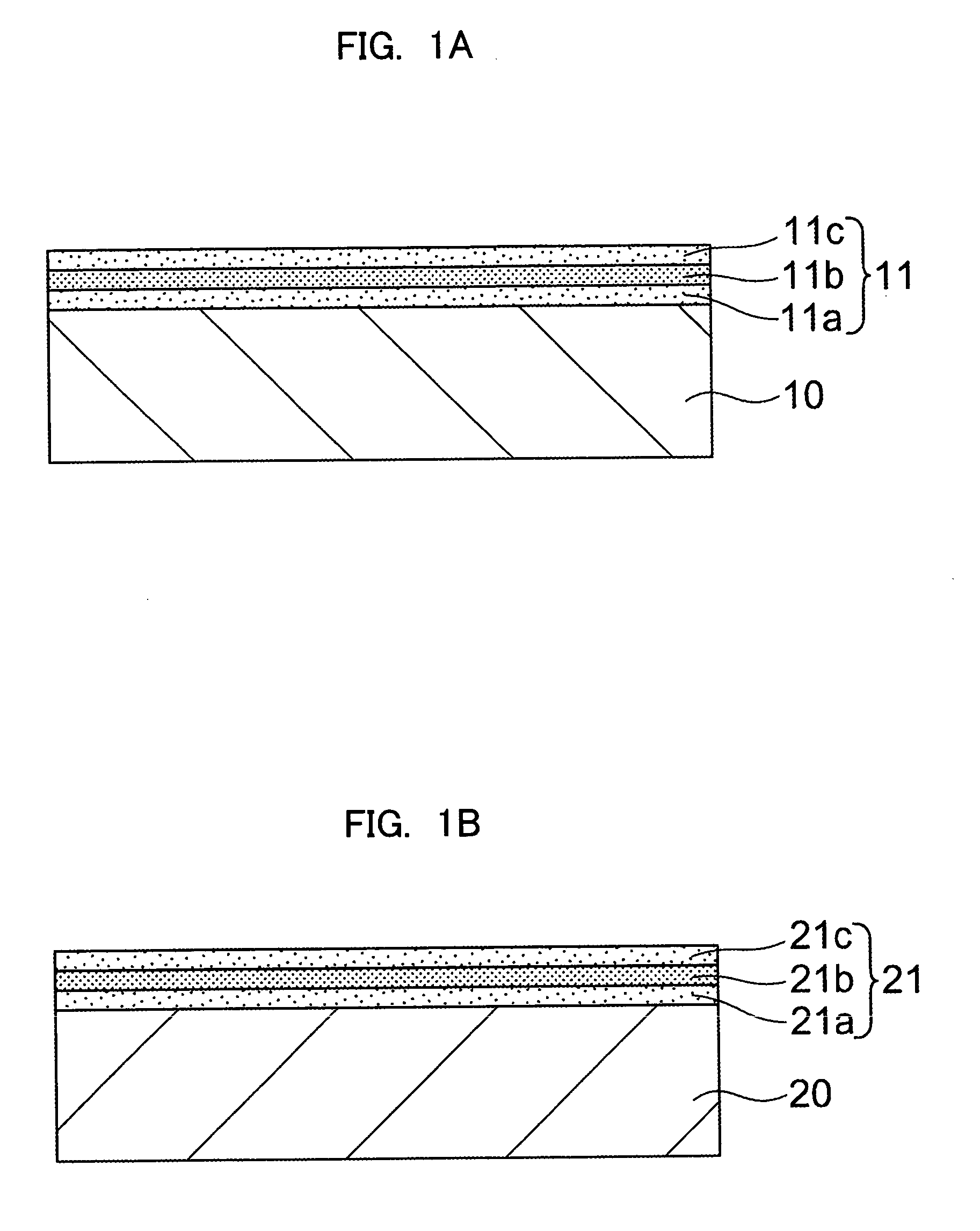
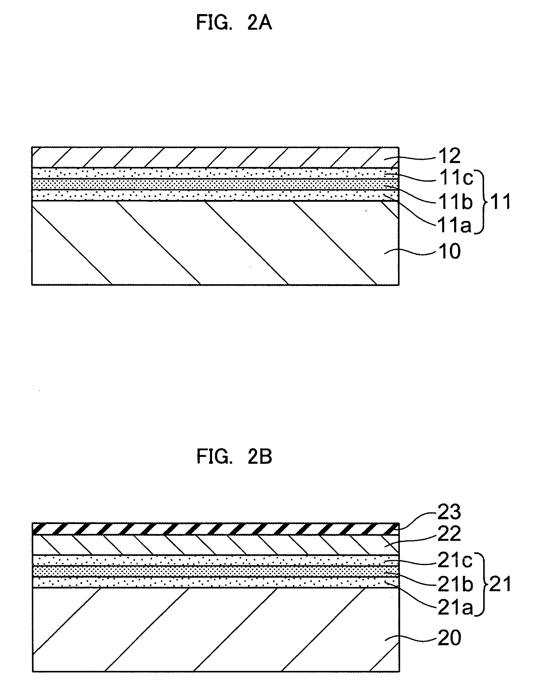
[0068] Step 1: Formation of Porous Layer

[0069] In this step, a porous Si layer is formed on a seed wafer (hereinafter referred to as a “seed substrate”) and a handle wafer (hereinafter referred to as a “support substrate”) by anodization. At this time, in order to facilitate separation of the seed substrate, a thickness and porosity of the high porous Si layer on the seed substrate are formed larger than those...

second embodiment

[0194] Second Embodiment

[0195] In the present embodiments, the explanation will be given of a method of production and production apparatus of a back-illuminated solid-state image pickup device of a single-surface resin sealed ultra-thin chip size hollow package using the double ion implanted layer separation method (the method of separating a seed substrate by a first ion implanted layer formed by implanting for example hydrogen atoms in the seed substrate and separating the support substrate by a second ion implanted layer formed by implanting for example hydrogen in the support substrate) among the methods of fabrication of new ultra-thin SOI substrates.

[0196] Step 1: Formation of Hydrogen Ion Implanted Layer

[0197] First, as shown in FIG. 10A, a seed substrate 10 made of p-type Si single crystal of 8 inch diameter and 800 μm thickness (resistivity of 0.01 to 0.02 Ωcm) is implanted with hydrogen ions to form an ion implanted layer 13. The depth of this ion implanted layer 13 fro...

third embodiment

[0241] Third Embodiment

[0242] In the present embodiment, the explanation will be given of a method of production and production apparatus of a back-illuminated solid-state image pickup device of a single-surface resin sealed ultra-thin chip size hollow package using the porous layer / ion implanted layer separation method combining the porous layer separation method and ion implanted layer separation method described above (the method of separating a seed substrate by an ion implanted layer formed by implanting hydrogen atoms in the seed substrate and separating the support substrate by a porous Si layer formed on the support substrate) among the methods of fabrication of new ultra-thin SOI substrates.

[0243] Step 1: Formation of Hydrogen Ion Implanted Layer

[0244] First, in the same way as in the second embodiment, as shown in FIG. 15A, a seed substrate 10 made of p-type Si single crystal of 8 inch diameter and 800 μm thickness (resistivity of 0.01 to 0.02 Ωcm) is implanted with hydr...


PUM


Abstract

A method for producing an ultra-thin semiconductor chip and an ultra-thin back-illuminated solid-state image pickup device utilizing a semiconductor layer formed on a support substrate via an insulating layer to improve separation performance of a semiconductor layer from a support substrate and thereby improve the productivity and quality. The method uses two porous peeling layers on opposite sides of a substrate to produce an ultra-thin substrate.

Description

BACKGROUND OF THE INVENTION [0001] 1. Field of the Invention [0002] The present invention relates to an ultra-thin semiconductor chip according to a new ultra-thin silicon-on-insulator (SOI) substrate production method, more particularly a method and an apparatus for producing a back-illuminated solid-state image pickup device for detecting light incident from a back side of the substrate of an ultra-thin single-surface resin sealed chip size hollow package according to the new ultra-thin SOI substrate production method. [0003] 2. Description of the Related Art [0004] For an image sensor having sensitivity with respect to an input of UV rays, soft X-rays, or an electron beam, use is being made of a back-illuminated charge coupled device (CCD) etc. [0005] Namely, UV rays, soft X-rays, and electron beams have a large absorption coefficient, so a CCD having no polycrystalline silicon electrodes or other obstacle at the incident surface, that is, a back-illuminated CCD illuminated from ...

Claims


Application Information

Patent Timeline
Patent Type & Authority Applications(United States)
IPC IPC(8): H01L21/00H01L27/14H01L21/46H01L23/00H01L27/146H01L27/148
CPCH01L27/14618H01L27/1464H01L27/14627H01L27/14634H01L27/14636H01L27/14643H01L27/14685H01L27/14687H01L27/14692H01L27/14837H01L27/14843H01L27/14621H01L2224/16225H01L2924/13091H01L2924/00H01L2224/45144H01L2224/05008H01L2224/05548H01L2224/05001H01L2224/05624H01L2924/00014H01L24/05H01L2224/05099H01L27/148H01L23/00
Inventor YAMANAKA, HIDEO
Owner SONY CORP
Why Eureka
Try Eureka