Electronic device, on-chip memory and method of operating the on-chip memory

An on-chip memory, electronic device technology, applied in instrumentation, electrical digital data processing, memory address/allocation/relocation, etc., can solve problems such as low-priority transaction delay, DRAM throughput reduction, etc., to reduce memory delay, Guarantees the effect of memory delay and stable communication

Inactive Publication Date: 2017-04-19
SAMSUNG ELECTRONICS CO LTD
View PDF5 Cites 1 Cited by
  • Summary
  • Abstract
  • Description
  • Claims
  • Application Information

AI Technical Summary

Problems solved by technology

When using this method, the latency of low-priority transact

Method used


Image

  • Electronic device, on-chip memory and method of operating the on-chip memory
  • Electronic device, on-chip memory and method of operating the on-chip memory
  • Electronic device, on-chip memory and method of operating the on-chip memory

Examples


Embodiment Construction

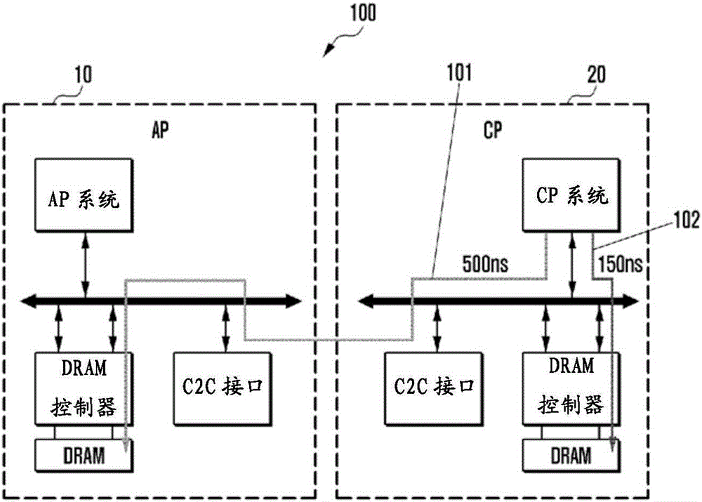
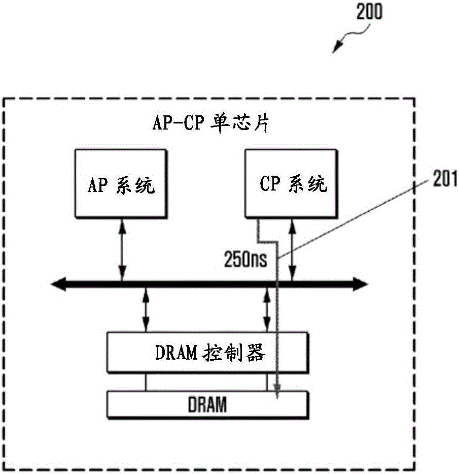
[0040] In this patent document, the terms used to describe the principles of the disclosure Figure 3 to Figure 20 , the following discussion, and the various examples are by way of illustration only and should not be construed in any way as limiting the scope of the present disclosure. Those skilled in the art will understand that the principles of the present disclosure may be implemented in any suitably arranged wireless communication device. Hereinafter, embodiments of the present disclosure will be described in detail with reference to the accompanying drawings. It should be noted that the same reference numerals may denote the same components in the drawings. Further, detailed descriptions of known functions and configurations that may make the subject matter of the present disclosure unclear will be omitted.

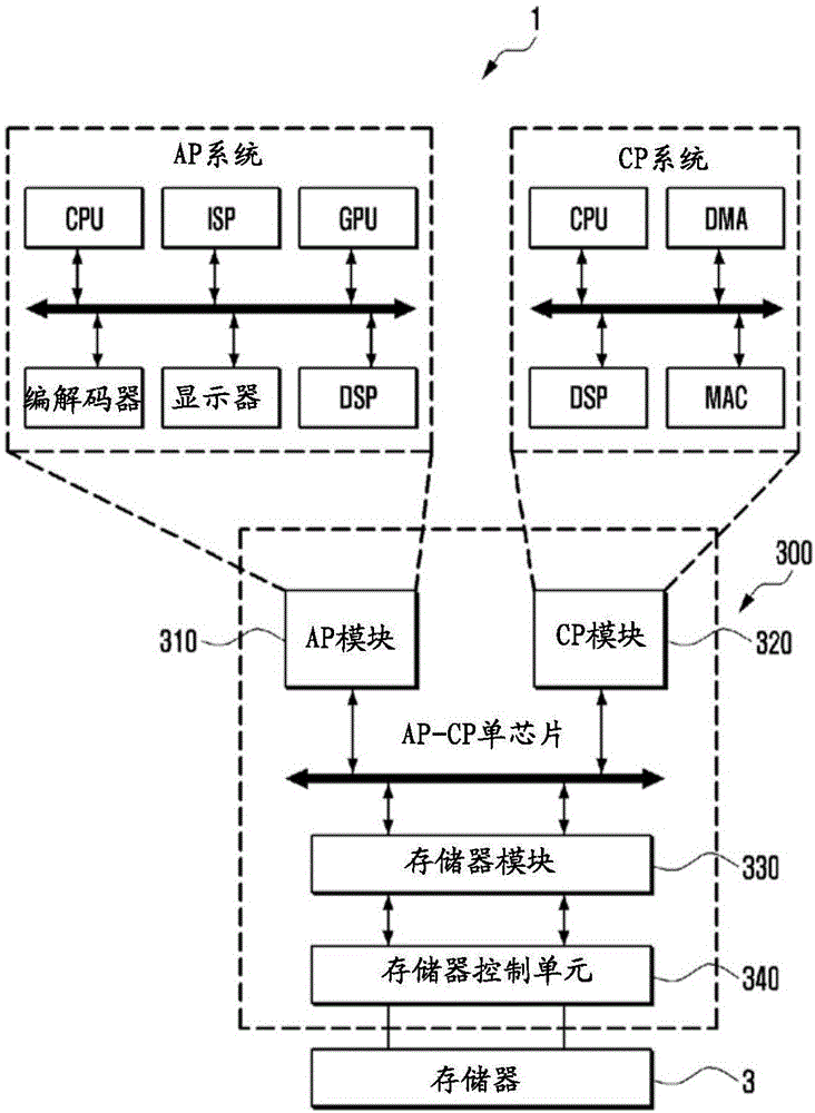
[0041] image 3 is a block diagram illustrating configurations of various embodiments of an electronic device according to the present disclosure.

[0042] re...


PUM


Abstract

An electronic device, an on-chip memory and a method of operating the on-chip memory are disclosed. The on-chip memory including an on-chip memory comprises: a plurality of design Intellectual Property (IPs), a memory that includes a storage area and a processor connected to the memory, wherein the processor is configured to monitor a memory traffic of at least one IP among the plurality of design IPs, and control usage of a storage area based on a result of the monitoring. According to the electronic device, the on-chip memory and the method of operating the on-chip memory of the present disclosure, in an AP-CP one chip structure, a stable communication is secured, memory latency is secured for a code required to process a real time of a CP, and in the AP-CP one chip structure, a communication bandwidth is improved.

Description

technical field [0001] The present disclosure relates to an electronic device, an on-chip memory, and a method of operating the same, and more particularly, to an on-chip memory in which an application processor, a communication processor, and a memory are mounted on a single chip, and an operation method of the chip memory. Background technique [0002] In the mobile environment, application processors (APs) are widely used in mobile devices such as smart phones and tablet devices. The competition for high performance, diverse functions, and miniaturization in size of mobile devices has become fierce. In light of this competition, there is an ongoing effort to reduce size and cost by including a communications processor (CP) in the AP, which is formed as an add-on chip and connected to the AP. [0003] figure 1 and figure 2 It is a view showing the AP-CP connection structure. [0004] refer to figure 1 and figure 2 , in the AP-CP single chip 200, memory latency inc...

Claims


Application Information

Patent Timeline
IPC IPC(8): G06F12/02G06F11/30
CPCG06F21/79G06F3/0604G06F3/0653G06F3/0673
Inventor 黄赞荣梁承珍
Owner SAMSUNG ELECTRONICS CO LTD
Why Eureka
Try Eureka