Circuit board testing device

A test device and circuit board technology, applied in the test field, can solve problems such as deformation of PIN feet, unacceptable by customers, and influence on product appearance, etc., and achieve the effect of small pressure/pressure and good test results

Inactive Publication Date: 2017-04-26
SHENZHEN YANMADE TECH CO LTD
View PDF4 Cites 10 Cited by
  • Summary
  • Abstract
  • Description
  • Claims
  • Application Information

AI Technical Summary

Problems solved by technology

[0002] In the circuit board testing device of the prior art, when the probes are in contact with the PIN pin of the connector of the circuit board to be tested, it is easy to leave a pin point on the PIN pin, or cause the PIN pin to deform, or even pierce the PIN pin and damage the circuit. Not only will it affect the appearance of the product, making it unacceptable to customers, but it will also cause abnormalities in the function of the circuit board to be tested.

Method used


Image

  • Circuit board testing device
  • Circuit board testing device
  • Circuit board testing device

Examples


Embodiment 1

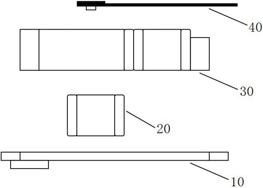
[0015] Such as figure 1 As shown, the circuit board testing device of this embodiment includes an adapter module 10, a conductive module 20, a support module 30 and a control unit (not shown in the figure).

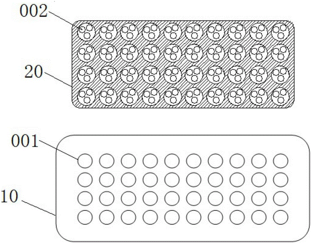
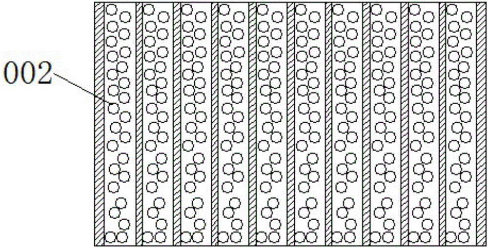
[0016] Such as figure 2 As shown, the adapter module 10 is provided with several test points 001, and each test point is used to collect an electrical connection pin of the device on the circuit board under test. Several conductive pathways 002 of the conductive module 20; the bottom surface of the conductive module 20 is connected to the adapter module 10, so that a number of test points of the adapter module 10 are electrically connected with a plurality of conductive pathways of the conductive module 20; the top surface of the conductive module 20 is used for contacting Test the circuit board, so that the conductive path of the conductive module 20 is electrically connected to the electrical connection pins of the device on the tested circuit board in one-to-one corr...


PUM


Abstract

The invention discloses a circuit board testing device which comprises a switching module, a conductive module, a supporting module and a control unit. The switching module is provided with a plurality of testing points. The bottom surface of the conductive module is connected with the switching module so that the plurality of testing points of the switching module are electrically connected with a plurality of conductive paths of the conductive module in a one-to-one correspondence manner. The top surface of the conductive module is used for making contact with a to-be-tested circuit board so that the conductive paths of the conductive module are electrically connected with electric connecting pins of a device on the tested circuit board in a one-to-one correspondence manner. According to the circuit board testing device, the conductive module realizes electric connection between the testing points of the switching module and pins of a to-be-tested product through the plurality of conductive paths, thereby realizing a good testing effect. Furthermore compared with a prior-art probe, the conductive module has advantages of lower pressure in making contact with the pins of the product, and effective prevention for pressing damage, stab and deformation of pins of the product.

Description

technical field [0001] The present application relates to the testing field, in particular to a circuit board testing device. Background technique [0002] In the circuit board testing device of the prior art, when the probes are in contact with the PIN pin of the connector of the circuit board to be tested, it is easy to leave a pin point on the PIN pin, or cause the PIN pin to deform, or even pierce the PIN pin and damage the circuit. Not only will it affect the appearance of the product, causing customers to be unacceptable, but it will also cause abnormalities in the realization of the function of the circuit board to be tested. Contents of the invention [0003] The invention provides a circuit board testing device, which includes a transfer module and a conductive module; a plurality of test points are arranged on the transfer module, and each test point is used to collect an electrical connection pin of a device on the circuit board to be tested; The conductive mod...

Claims


Application Information

Patent Timeline
Patent Type & Authority Applications(China)
IPC IPC(8): G01R31/28
CPCG01R31/2808
Inventor 黄丁
Owner SHENZHEN YANMADE TECH CO LTD
Why Eureka
Try Eureka