Test system of semiconductor laser chip

A test system and laser technology, which is applied in electronic circuit testing, integrated circuit testing, instruments, etc., can solve the problems of semiconductor laser chip loss and inestimable loss, and achieve the effect of avoiding accidental failure and reducing loss

Pending Publication Date: 2017-04-26
RESEARCH INSTITUTE OF TSINGHUA UNIVERSITY IN SHENZHEN +1
View PDF9 Cites 7 Cited by
  • Summary
  • Abstract
  • Description
  • Claims
  • Application Information

AI Technical Summary

Problems solved by technology

[0004] The aging test and long-term life test at a specific current, power, and temperature have very high requirements for the test system. For the aging test, if there is an accidental death of the semiconductor laser chip caused by the test system, it will cause a lot of losses. , and for the long-term life test process, if an accident occurs, the entire life test will be wasted, and the loss is immeasurable

Method used


Image

  • Test system of semiconductor laser chip
  • Test system of semiconductor laser chip
  • Test system of semiconductor laser chip

Examples


Embodiment Construction

[0046] The present invention will be described in detail below in conjunction with the accompanying drawings and embodiments.

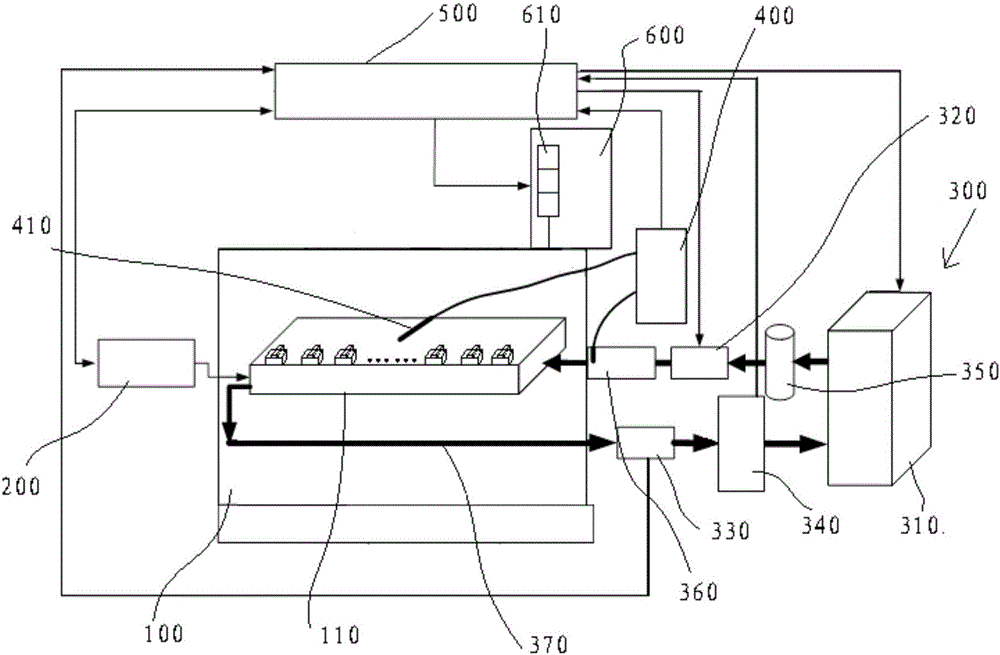
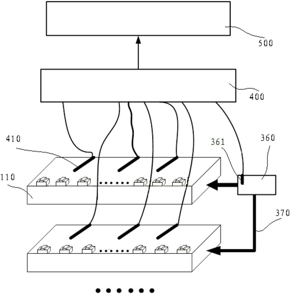
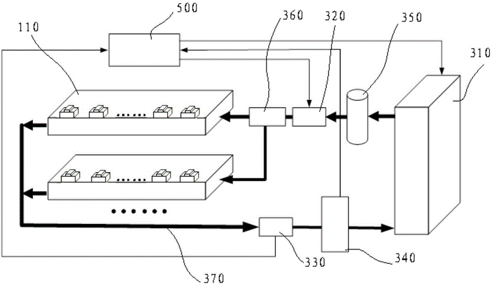
[0047] Such as figure 1 , a test system for a semiconductor laser chip according to an embodiment of the present invention, the test system can be used for aging test and life test of the chip, and can also be used for other tests of the chip; the test system includes a test cabinet 100, a test power supply 200, and a cooling subsystem 300 , temperature monitoring subsystem 400 and computer processing subsystem 500 .

[0048] The test cabinet 100 can provide a relatively airtight test environment to reduce the influence of external interference factors in the test process; the test cabinet 100 includes a loading platform 110, and a plurality of chip components to be tested are placed on the loading platform 110; by setting the loading platform 110 , placing a plurality of chip components to be tested on the loading platform 110 can realize simultaneo...


PUM


Abstract

The invention discloses a test system of a semiconductor laser chip. The system comprises a test cabinet, a test power supply, a cooling subsystem, a temperature monitoring subsystem and a computer processing subsystem. The test cabinet comprises a loading platform. A plurality of chip components to be tested are placed on the loading platform. The test power supply is used for providing a test current for the plurality of chip components to be tested. The cooling subsystem is used for providing a circulated cooling liquid for the loading platform so as to provide a stable and reliable temperature for chip component tests. The temperature monitoring subsystem is used for monitoring temperatures of the loading platform and the circulated cooling liquid. The computer processing subsystem is used for making the cooling subsystem provide the circulated cooling liquid possessing the stable and reliable temperature and emitting a corresponding control instruction to the test power supply according to a result monitored by the temperature monitoring subsystem. Through the above mode, test safety can be increased and losses brought by accidental failure of the semiconductor laser chip components are avoided.

Description

technical field [0001] The invention relates to the technical field of testing semiconductor laser chips, in particular to a testing system for semiconductor laser chips. Background technique [0002] With the rapid development of emerging fields such as laser display, laser lighting, 3D printing, and space-ground integrated network, the market for high-power semiconductor lasers is gradually expanding, and the high demand for high-power semiconductor lasers has brought about a huge demand for upstream semiconductor laser chips. , the requirements for output power and reliability of semiconductor laser chips are also increasing. [0003] In order to test effectively, it is necessary to package the semiconductor laser chip on a heat sink with high thermal conductivity, referred to as the semiconductor laser chip component, which is convenient for the subsequent secondary integrated packaging design, such as optical fiber coupling. The common form of chip packaging is COS (Ch...

Claims


Application Information

Patent Timeline
Patent Type & Authority Applications(China)
IPC IPC(8): G01R31/28
CPCG01R31/286G01R31/2891
Inventor 胡海刘文斌王泰山李成鹏方继林
Owner RESEARCH INSTITUTE OF TSINGHUA UNIVERSITY IN SHENZHEN
Why Eureka
Try Eureka