
Nano light-emitting array, manufacturing method thereof, and nano light-emitting device

A light-emitting array and nanorod array technology, which is applied in semiconductor/solid-state device manufacturing, semiconductor devices, electrical components, etc., can solve the problems of limited piezoelectric sensors, limited sensor manufacturing, and insufficient application of flexible devices.

Active Publication Date: 2019-05-17
BEIJING INST OF NANOENERGY & NANOSYST
View PDF10 Cites 0 Cited by
  • Summary
  • Abstract
  • Description
  • Claims
  • Application Information

AI Technical Summary

Problems solved by technology

However, such heterojunction LED arrays based on patterned ZnO nanowires still have significant limitations.
Firstly, there are few types of inorganic semiconductor nanomaterials, especially the p-type material used as hole transport, which limits the manufacture of the sensor; secondly, the flexibility of inorganic nanomaterials is poor, and their applications in flexible devices are limited. insufficient
These two points greatly limit the development of piezoelectric sensors based on ZnO nanowire piezoelectric photoelectronics effect, especially the development and application of large-area flexible array devices.

Method used


Image

  • Nano light-emitting array, manufacturing method thereof, and nano light-emitting device
  • Nano light-emitting array, manufacturing method thereof, and nano light-emitting device
  • Nano light-emitting array, manufacturing method thereof, and nano light-emitting device

Examples


Embodiment approach

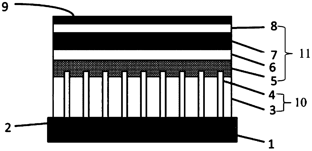
[0042] According to one embodiment of the present invention, the nano-luminescence control layer 10 may include a nanowire or nanorod array 4 and a dielectric material layer 3 formed by filling the gaps of the nanowire or nanorod array with a transparent dielectric material. , wherein the material of the nanowire or nanorod array 4 may be a piezoelectric material.

[0043] According to an embodiment of the present invention, the piezoelectric material may be a wurtzite structure material, preferably gallium nitride, gallium arsenide or zinc oxide (ZnO). The transparent dielectric material can be polymer or silicon oxide.

[0044] According to one embodiment of the present invention, in the nanowire or nanorod array 4, each array unit is a nanowire cluster or a nanorod cluster, and the diameter of each array unit may range from 100nm to 5um. The length of the nanorods can range from 1um to 10um, and the gap between two adjacent array units can range from 2um to 200um.

[0045...


PUM

PropertyMeasurementUnit
diameteraaaaaaaaaa
thicknessaaaaaaaaaa
thicknessaaaaaaaaaa

Abstract

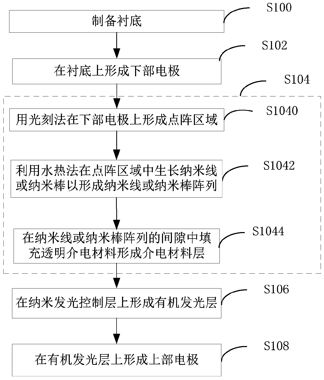
The invention relates to the field of micro-nano energy technology, and discloses a nano-luminescent array, a manufacturing method thereof, and a nano-luminescent device. Wherein, the nano-luminescence array includes: a substrate; a lower electrode formed on the substrate; a nano-luminescence control layer formed on the lower electrode; an organic light-emitting layer formed on the nano-luminescence control layer; The upper electrode is formed on the organic light emitting layer. By using the above-mentioned nano-luminescence array and nano-luminescence device of the present invention, the nano-luminescence control layer can obtain the stress information applied on the layer, so that it can quickly respond to the applied stress, and then realize the control of the organic light-emitting layer. Adjustment of luminous intensity.

Description

technical field [0001] The invention relates to the field of micro-nano energy technology, in particular to a nano-luminescent array, a manufacturing method thereof, and a nano-luminescent device. Background technique [0002] Pressure sensors based on the piezoelectric effect of ZnO nanowires have attracted great interest in recent years. The piezoelectric electronic effect is used to control the generation, transport, separation or recombination of carriers, thereby improving the performance of optoelectronic devices. [0003] For example, a pressure sensor based on the piezoelectric electronics effect of arrayed ZnO nanowires in the prior art can improve the resolution to 120 microns. Another pressure sensor sensor based on p-type gallium nitride layer epitaxial patterned growth of ZnO nanowire light-emitting diode arrays has achieved a resolution of 2.7 microns, which is the first stress sensing system in the world to achieve micron-level superhuman skin resolution. Th...

Claims


Application Information

Patent Timeline
Patent Type & Authority Patents(China)
IPC IPC(8): H01L27/32H01L21/77
CPCH01L21/77H10K59/00
Inventor 潘曹峰鲍容容王春枫董林
Owner BEIJING INST OF NANOENERGY & NANOSYST
Learn More