

A kind of magnetron sputtering table and magnetron sputtering device
A magnetron sputtering and substrate technology, which is applied in sputtering coating, metal material coating process, vacuum evaporation coating and other directions, can solve the problems of low adjustment accuracy of the substrate to be formed and the mask plate, etc.
- Summary
- Abstract
- Description
- Claims
- Application Information
AI Technical Summary
Problems solved by technology
Method used
Image

Examples
Embodiment Construction
[0032] The following will clearly and completely describe the technical solutions in the embodiments of the present invention with reference to the accompanying drawings in the embodiments of the present invention. Obviously, the described embodiments are only some, not all, embodiments of the present invention. Based on the embodiments of the present invention, all other embodiments obtained by persons of ordinary skill in the art without making creative efforts belong to the protection scope of the present invention.
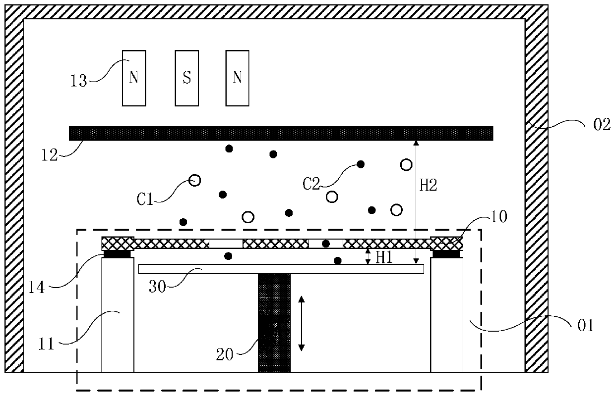
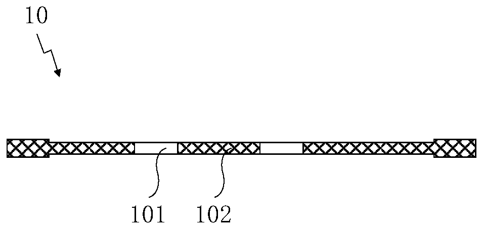
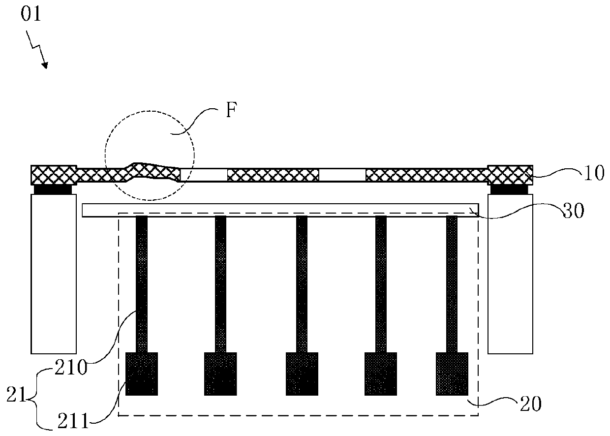
[0033] Embodiments of the present invention provide a figure 1 Magnetron sputtering station 01 shown. The magnetron sputtering station 01 includes a mask plate 10 , a lifting mechanism 20 and a substrate 30 to be filmed. Wherein, the mask plate 10 such as figure 2 As shown, there are opening regions 101 and shielding regions 102 arranged at intervals.
[0034] Specifically, the substrate 30 to be filmed is located on the carrying surface of the lifting mec...
PUM
 Abstract
Description
Claims
Application Information