Display device

A display device and display panel technology, which is applied in optics, instruments, electrical digital data processing, etc., can solve the problem of low image accuracy of texture recognition, and achieve the effect of improving accuracy and clarity and improving recognition rate.

Active Publication Date: 2017-05-31
BOE TECH GRP CO LTD
View PDF5 Cites 130 Cited by
  • Summary
  • Abstract
  • Description
  • Claims
  • Application Information

AI Technical Summary

Problems solved by technology

[0004] In view of this, an embodiment of the present invention provides a display device to solve the problem of low accuracy of existing texture recognition images

Method used


Image

  • Display device
  • Display device
  • Display device

Examples


Embodiment 1

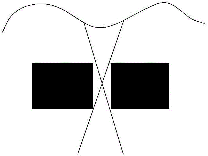
[0045] Embodiment 1: the arrangement of the first light collimation member 410 .

[0046] In specific implementation, in the above-mentioned display device provided by the embodiment of the present invention, the display panel 100 can specifically adopt the following Figure 4a to Figure 4d The electroluminescent display panel shown can also be used as Figure 5a to Figure 5b The LCD panel shown.

[0047] When the display panel adopts an electroluminescence display panel, such as Figure 4a to Figure 4d As shown, the display panel 100 specifically includes: a base substrate 110, a pixel control circuit device 120 disposed on the base substrate 110, a plurality of light emitting elements 130 disposed on the pixel control circuit device 120, and a cover light emitting element 130 The encapsulation film 140; wherein, the pixel control circuit device 120 is composed of a plurality of thin film transistors, and only one thin film transistor is schematically shown in the figure. ...

Embodiment 2

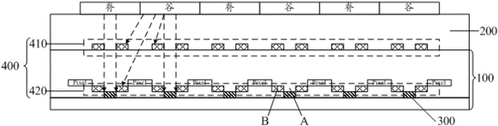
[0059] Embodiment 2: the arrangement of the second light collimation member 420 .

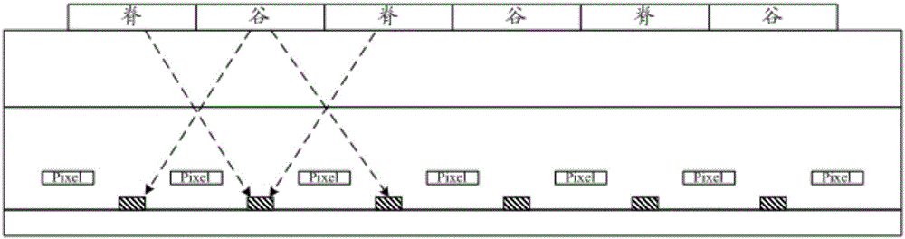
[0060] When the display panel adopts an electroluminescence display panel, in the above-mentioned display device provided by the embodiment of the present invention, as Figure 4a to Figure 4d As shown, the second light collimating member 420 may include: one or a combination of the gate film layer 121 and the source-drain film layer 122 in the pixel control circuit device 120, and the anode layer 131 in the light emitting element 130 is arranged in the same layer The light-shielding member has a light-shielding area in the non-light-emitting area where the photosensitive device 300 is disposed, and has a light-transmitting area above the photosensitive device 300 .

[0061] exist Figure 4a with Figure 4b shows a case where a light-shielding component is set in the same layer as the source-drain film layer 122, in Figure 4c shows the case where two light-shielding components are respectiv...

Embodiment 3

[0064] Embodiment 3: The photosensitive device 300 is disposed in the non-display area of ​​the display panel 100 .

[0065] Furthermore, when the photosensitive device 300 is arranged in the non-light-emitting area of ​​the display area of ​​the display panel 100, the light-shielding area B must not be set in the opening area of ​​the pixel unit Pixel by the light-collimating member 400, so it is inevitable that stray light will be incident to the photosensitive device 300 . In the case of a high requirement for the definition of texture recognition, during specific implementation, in the above-mentioned display device provided by the embodiment of the present invention, the photosensitive device may also be arranged in the non-display area of ​​the display panel.

[0066] Taking the liquid crystal display panel as an example for the display panel, in the above-mentioned display device provided by the embodiment of the present invention, as Figure 5b As shown, the first lig...


PUM


Abstract

The invention discloses a display device. The device comprises a display panel with a plurality of pixel units, a protective cover plate arranged on a light-out surface of the display panel, a plurality of photosensitive devices arranged at one side of the pixel unit opposite to the light-out surface and used for line recognition, an optical collimator arranged between the protective cover plate and the plurality of photosensitive devices is added, the optical collimator is provided with a transmittance area on the top of the photosensitive devices, the remaining area except for the transmittance area is a shading area, part of stray light adjacent to a ridge and display luminescence given out by the pixel units and entering the photosensitive devices can be filtered by the shading area, the transmittance area can ensure that the ridge reflected light enters the corresponding photosensitive devices, the line recognition rate of the photosensitive devices is improved, and therefore the precision and definition of line recognition images are improved.

Description

technical field [0001] The present invention relates to the field of display technology, in particular to a display device. Background technique [0002] At present, the devices that realize the texture recognition function installed on display devices such as mobile phones are all in non-display areas such as the home button or the back of the display device, and the future development direction of display devices is ultra-thin, high color gamut, wide viewing angle and integrated Various sensing functions. When the optical sensor (Sensor) that realizes texture recognition is integrated inside the display panel, the distance between the Sensor and the finger contact surface will increase, causing the distance for the reflected light from the finger to reach the Sensor to increase, and the light reflected by the finger will reach the Sensor. Scattering occurs before the Sensor, such as figure 1 As shown, a single optical sensor receives fingerprint information of multiple v...

Claims


Application Information

Patent Timeline
Patent Type & Authority Applications(China)
IPC IPC(8): G02F1/1333G06K9/00
CPCG02F1/13338G06V40/1324G02F1/13471G02F1/157G06F3/0421G02F2201/44G06F3/0445G02F1/155G02F1/134309G02F1/133512G02F1/13318G02F1/163G02F1/13312
Inventor 王海生刘英明丁小梁许睿赵利军贾亚楠顾品超秦云科郭玉珍韩艳玲吴俊纬李昌峰董学
Owner BOE TECH GRP CO LTD
Why Eureka
Try Eureka