Built-in touch panel and display device

A touch panel and display device technology, which is applied in optics, instruments, electrical digital data processing, etc., can solve problems affecting pixel aperture ratio, and achieve the effects of avoiding uneven liquid crystal alignment, improving production efficiency, and increasing aperture ratio

Active Publication Date: 2017-05-31
WUHAN CHINA STAR OPTOELECTRONICS TECH CO LTD
View PDF5 Cites 3 Cited by
  • Summary
  • Abstract
  • Description
  • Claims
  • Application Information

AI Technical Summary

Problems solved by technology

[0006] The present invention aims at the problem that a large-area black matrix is ​​set around the spacer in the built-in touch panel, thereby affecting the pixel aperture ratio, and proposes a built-in touch panel. At the same time, the built-in touch panel proposed by the present invention is because the spacer is arranged on the conductive line , so that it will not affect the density of the spacers and will not affect the thickness of the LCD panel

Method used


Image

  • Built-in touch panel and display device
  • Built-in touch panel and display device
  • Built-in touch panel and display device

Examples


Embodiment 1

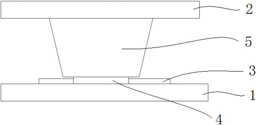
[0040] Figure 4a For Embodiment 1 of the present invention, Figure 4b for Figure 4a A sketch of the combined Figure 4a and Figure 4b , the shape of the first projection 15 of the first contact surface of the spacer on the conductive line 14 is rectangular, and the conductive line 14 at the first projection 15 is continuous. Figure 4a In the X direction and the Y direction, respectively, in the X direction, the width of the first projection 15 is equal to or smaller than the width of the conductive line 14, and the first projection 15 extends along the Y direction, so the first projection 15 is completely located on the conductive line 14, that is, the spacer completely stands on the conductive wire 14 through the first contact surface. In FIG. set as Figure 5a Oval 25 in or as Figure 5b The oblong circle 35 in the center, this setting can ensure that the area of ​​the first projection on the conductive wire 14 is the same as the design value, ensuring the support...

Embodiment 2

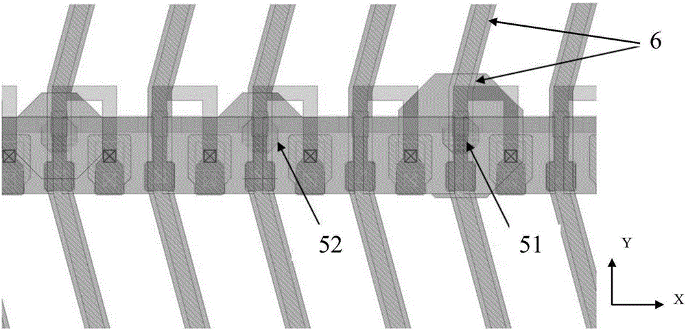
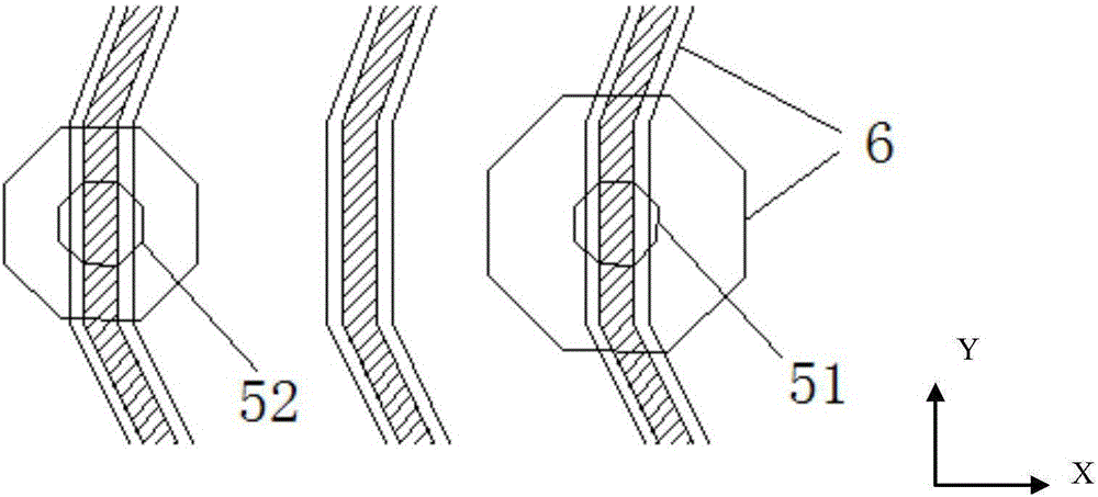
[0045] Figure 9a For the second embodiment of the present invention, Figure 9a is the view along the normal direction of the panel, Figure 9b for Figure 9a sketch of Figure 10 It is the sectional view of this embodiment. The difference between embodiment two and embodiment one is that in Figure 10 In, the thickness of the conductive wire 49 is greater than the first thickness in the first embodiment, in Figure 9a In the X direction and the Y direction, respectively, in the X direction, the width of the second contact surface 65 of the spacer is larger than the width of the conductive line 49, and the area of ​​the second contact surface 65 is larger than that of the second contact surface in Embodiment 1. area, so that the spacer 59 rides on the conductive line 49, such as Figure 10 As shown, it helps the stability of the spacer 59, but the contact area between the spacer 59 and the conductive line 49 is still equal to the contact area in Embodiment 1. Since the t...


PUM


Abstract

The invention relates to the field of liquid crystal display panels, and provides a built-in touch panel. The wire at a spacer is consecutive, the total area where the bottom face of the spacer makes contact with the wire is not changed, by changing the shape of the bottom face of the spacer, the spacer totally stands on the wire, thereby in the process of thinning or pressing the panel, the spacer is not in contact friction with aligned film around the wire, likewise, by changing the thickness of the wire, the gap between the bottom face of the spacer standing on the wire and the top face of the aligned film is increased, the situation that in the process of thinning or pressing the panel, the spacer is in contact friction with the aligned film, and large-area uneven orientation of liquid crystal is further avoided, thus, the area of a black matrix arranged around the spacer is greatly reduced, and the aperture ratio of a pixel is increased.

Description

technical field [0001] The invention relates to the technical field of liquid crystal panel display, in particular to a built-in touch panel and a display device capable of reducing image display unevenness. Background technique [0002] The built-in touch panel refers to the method of embedding the touch panel function into the LCD pixels. Compared with the traditional external LCD panel, the thickness of the built-in touch panel is smaller. [0003] figure 1 It is a sectional view of an existing liquid crystal display panel, which generally includes a first substrate, a second substrate, and a liquid crystal layer (not shown) sealed between the first substrate and the second substrate, from figure 1 It can be seen from the figure that the liquid crystal panel includes a first substrate 1, a second substrate 2, an alignment film 3, conductive lines 4, and spacers 5, and the spacers 5 determine the thickness of the liquid crystal panel, thereby determining the response time...

Claims


Application Information

Patent Timeline
Patent Type & Authority Applications(China)
IPC IPC(8): G02F1/1339G02F1/1333G06F3/041
CPCG02F1/13338G02F1/13394G06F3/0412G02F2201/40G02F1/13398G02F1/1337G02F1/133512
Inventor 张春倩王超陈归
Owner WUHAN CHINA STAR OPTOELECTRONICS TECH CO LTD
Why Eureka
Try Eureka