SSD master control BE Buffer, SSD master control, data transmission management device and data transmission management method

A technology of data transmission and management device, which is applied in electrical digital data processing, input/output process of data processing, input/output to record carrier, etc., and can solve the problems of large IO transmission efficiency deterioration, long invalid waiting time between DMAs, etc. , to achieve the effect that the transmission efficiency will not deteriorate, the invalid waiting time will be reduced, and the CPU time resources will be saved.

Active Publication Date: 2017-05-31
HUNAN GOKE MICROELECTRONICS
View PDF11 Cites 7 Cited by
  • Summary
  • Abstract
  • Description
  • Claims
  • Application Information

AI Technical Summary

Problems solved by technology

[0020] The technical problem to be solved by the present invention is to provide a BE Buffer for SSD main control, SSD main control, and data transmission management device and method for the deficiencies of the existing technology, so as to solve the problem that CPU time resources are relatively small in the existing DMA data transmission management method. Multiple, invalid waiting time between DMAs is too long, and large IO transmission efficiency deteriorates, reducing the occupation of CPU time resources, improving data transmission efficiency between DMAs, reducing invalid delays, and ultimately improving SSD data throughput

Method used


Image

  • SSD master control BE Buffer, SSD master control, data transmission management device and data transmission management method
  • SSD master control BE Buffer, SSD master control, data transmission management device and data transmission management method
  • SSD master control BE Buffer, SSD master control, data transmission management device and data transmission management method

Examples


Embodiment Construction

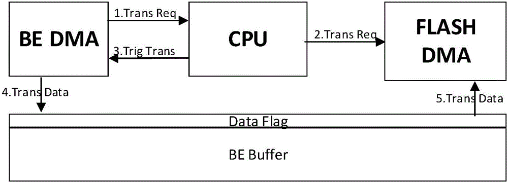
[0039] Such as image 3 , the realization process of the present invention is as follows:

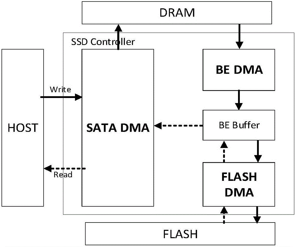
[0040] 1. Agree on the specified size of the storage unit and the Data Flag space. The Buffer between DMAs is composed of multiple storage units. Each storage unit has its own 1-bit or multi-bit information corresponding to it in the Data Flag. If the Data Flag of a certain storage unit is in state 0, it means that the storage unit is not full; if the Data Flag of a certain storage unit is in state 1, it means that the data in this storage unit is full. as in image 3 The agreed storage unit is 512B in size, and each storage unit has its own 1-bit information corresponding to it in the Data Flag. Status 0 indicates that the Data Flag value of the storage unit is 0, and status 1 indicates that the Data Flag value of the storage unit is 0. Buffer between DMAs is BE Buffer.

[0041] 2. On the basis of 1, when Write DMA needs to write a storage unit in the buffer, if its Data Flag is in st...


PUM


Abstract

The invention discloses an SSD master control BE Buffer, SSD master control, a data transmission management device and a data transmission management method. Buffer distribution, data synchronization and Buffer release in a DMA intertransmission process are completed automatically through DMA transmission control rules achieved by combination of a Data Flag and hardware, so that a CPU does not need to intervene a whole transmission process, and a great number of CPU time resources are saved; a great amount of Flash DMA waiting time is shortened, so that read delay is reduced. Particularly, aiming at high IO conditions, under the DMA transmission control rules achieved by combination of the Data Flag and the hardware, BE DMA/Flash DMA can achieve multiple times of transmission automatically by means of hang-up and wakeup according to Data Flag setting conditions without CPU intervention, so that transmission efficiency is improved instead of deteriorating under high IO scenes.

Description

technical field [0001] The invention relates to the field of SSD master control data transmission, in particular to an SSD master control BE Buffer, SSD master control, data transmission management device and method. Background technique [0002] In the mainstream SSD master control, there are often Sata DMA, Flash DMA, BE DMA and other DMAs, such as figure 1 As shown in FIG. 2 , the solid line arrows in the figure indicate the data flow direction under the write operation, and the dotted line arrows indicate the data flow direction under the read operation. [0003] In the SSD writing process, Sata DMA is responsible for transferring data from HOST to DRAM outside the chip, CoreDMA is responsible for transferring data in DRAM to BE Buffer in the chip, and FlashDMA is responsible for transferring data in BE Buffer to Flash; In the SSD reading process, FLASH DMA is responsible for transferring FLASH data to BE Buffer, and SATADMA is responsible for transferring BE Buffer dat...

Claims


Application Information

Patent Timeline
Patent Type & Authority Applications(China)
IPC IPC(8): G06F3/06
CPCG06F3/061G06F3/0611G06F3/0638G06F3/0679
Inventor 李雷陈旭光杨万云周士兵彭鹏马翼田达海
Owner HUNAN GOKE MICROELECTRONICS
Why Eureka
Try Eureka