Display substrate, display panel and display device

A technology for display substrates and display panels, applied in static indicators, instruments, etc., can solve problems such as short circuit of test probes, performance testing, signal interference, etc., and achieve the effect of improving reliability and reducing impact

Active Publication Date: 2017-05-31
SHANGHAI TIANMA MICRO ELECTRONICS CO LTD +1
View PDF7 Cites 6 Cited by
  • Summary
  • Abstract
  • Description
  • Claims
  • Application Information

AI Technical Summary

Problems solved by technology

However, when the performance of the display panel needs to be tested after the display panel is prepared, the short-connected parts of the above-mentioned multiple wires should be disconnected. At this time, when the laser is used to cut the wires along the edge of the display panel, the wires will melt and splash , after the test probes are pressed onto the test pads, the test probes are likely to be in electrical contact with the molten and spattered wires, which can easily lead to a short circuit between adjacent test pads or adjacent test probes, thereby causing The signals interfere with each other, and even burn the test pad due to short circuit, which affects the test of the performance of the display panel

Method used


Image

  • Display substrate, display panel and display device
  • Display substrate, display panel and display device
  • Display substrate, display panel and display device

Examples


Embodiment Construction

[0020] The present invention will be further described in detail below with reference to the drawings and embodiments. It can be understood that the specific embodiments described here are only used to explain the present invention, but not to limit the present invention. In addition, it should be noted that, for ease of description, the drawings only show a part but not all of the structure related to the present invention.

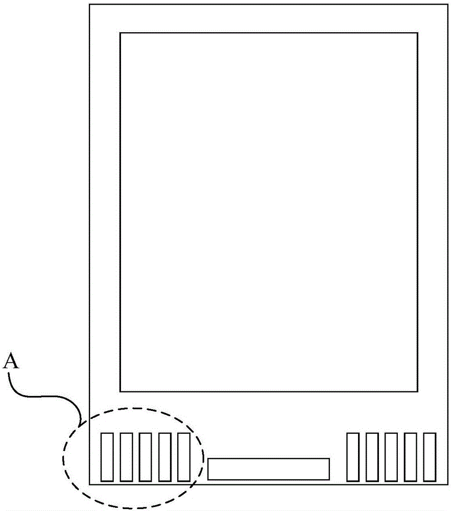
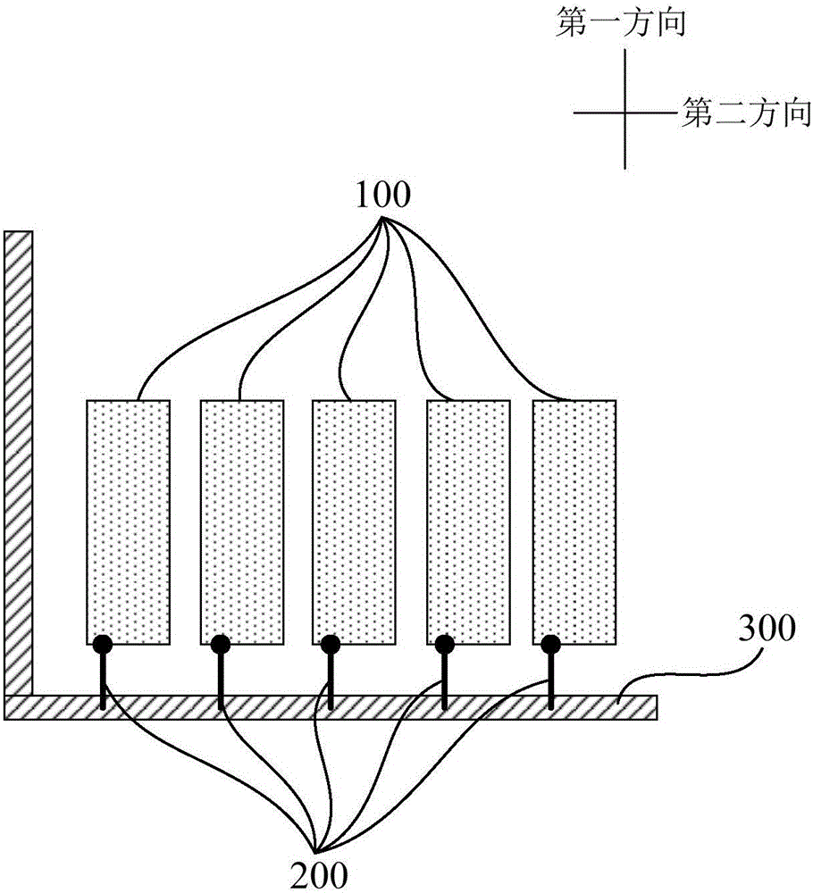
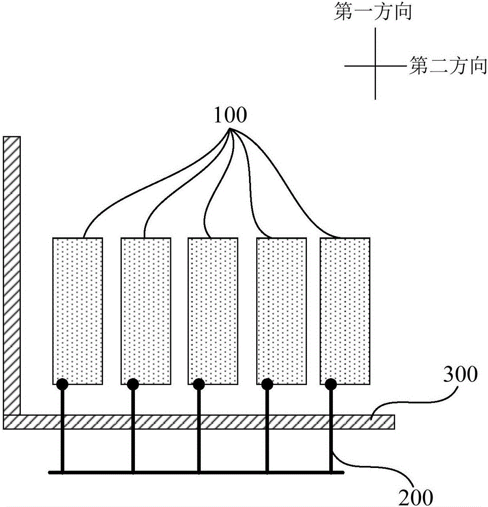
[0021] figure 1 Is a schematic structural diagram of a display substrate provided by an embodiment of the present invention; figure 2 for figure 1 Schematic diagram of the existing structure in Central A area. Such as figure 2 As shown, the display substrate may include a plurality of test pads 100 extending along a first direction and arranged along a second direction, the second direction being perpendicular to the first direction;

[0022] There are a plurality of anti-static traces 200 extending along the first direction to the edge 300 of the display ...


PUM


Abstract

The embodiment of the invention discloses a display substrate, a display panel and a display device. The display substrate comprises at least two test bonding pads which extend in a first direction and are distributed in a second direction, and multiple anti-static wires extending along the second direction to a first edge of the display substrate, wherein the second direction intersects with the first direction, and the anti-static wires are electrically connected with the test bonding pads correspondingly. Influences of molten and splashed wires on a testing unit are reduced, and the reliability of the testing unit is improved.

Description

Technical field [0001] The embodiments of the present invention relate to display technology, and in particular, to a display substrate, a display panel, and a display device. Background technique [0002] During the manufacturing process of the organic light emitting diode display panel or the liquid crystal display panel, after the display panel is prepared, the performance of the display panel needs to be tested. In the existing display panel design, in order to facilitate testing and good product screening, a test unit is generally set on the display substrate (such as an array substrate) of the display panel, and the performance test of the display panel is performed by inputting test signals to the test unit. [0003] Generally, the test unit includes a plurality of test pads arranged on the peripheral circuit area of ​​the array substrate. In the manufacturing process of the display panel, in order to prevent the generated static electricity from damaging the test pads, the ...

Claims


Application Information

Patent Timeline
Patent Type & Authority Applications(China)
IPC IPC(8): G09G3/00
CPCG09G3/006
Inventor 蔡晓波
Owner SHANGHAI TIANMA MICRO ELECTRONICS CO LTD
Why Eureka
Try Eureka