Array base plate, display panel and display device

A technology for array substrates and base substrates, which is applied in the field of display devices and can solve problems such as source and drain short circuits

Active Publication Date: 2017-08-18
BOE TECH GRP CO LTD +1
View PDF4 Cites 5 Cited by
  • Summary
  • Abstract
  • Description
  • Claims
  • Application Information

AI Technical Summary

Problems solved by technology

The array substrate includes a base substrate, a gate pattern layer, an active pattern layer and a source-drain pattern layer, the gate pattern layer includes a plurality of gate lines, the source-drain pattern layer includes a plurality of data lines, and a plurality of the The gate line and the plurality of data lines are intersected to divide the array substrate into a plurality of pixel units, the array substrate also includes thin film transistors arranged in the pixel units, and the gate pattern la

Method used


Image

  • Array base plate, display panel and display device
  • Array base plate, display panel and display device

Examples


Embodiment approach

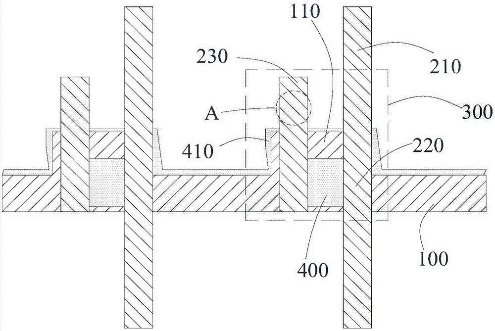
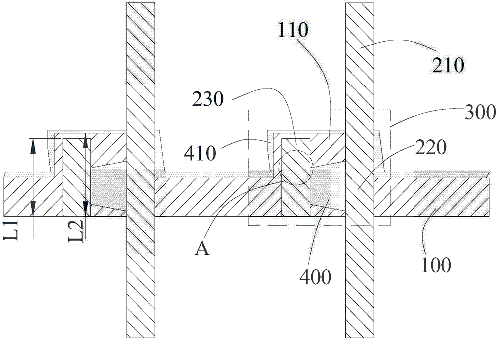
[0037] As a preferred implementation manner of the present invention, the common electrode can be arranged between the pixel electrode and the base substrate. Specifically, the array substrate includes a passivation insulating layer covering the source-drain pattern layer, the array substrate further includes a pixel electrode layer, and the pixel electrode layer has a plurality of pixel electrodes, and each of the pixel units is provided with One said pixel electrode, said pixel electrode is electrically connected to a corresponding drain through a via hole penetrating through said passivation insulating layer.

[0038] As a second aspect of the present invention, a display panel is provided, and the display panel includes an array substrate, wherein the array substrate is the above-mentioned array substrate provided by the present invention.

[0039] Since there is no residual active layer material between the source and the drain in the thin film transistor of the array sub...


PUM

PropertyMeasurementUnit
Lengthaaaaaaaaaa
Lengthaaaaaaaaaa

Abstract

The invention provides an array base plate. The array base plate comprises a under-laying base plate, a gate graphics layer, a source graphics layer and a source drain graphics layer, the gate graphics layer comprises multiple stripes of gate lines, the source drain graphics layer comprises multiple stripes of data lines, the gate lines and the data lines are arranged alternately, the array base plate is divided into multiple pixel units, the array base plate comprises a thin-film transistor arranged in the pixel units, the gate graphics layer comprises further a grid electrode of the thin film transistor, the source drain graphics layer comprises a source electrode and a drain electrode of the thin film transistor, the source graphics layer comprises an active layer of the thin-film transistor, wherein the orthographic projection of the drain electrode of the thin-film transistor on the under-laying base plate does not exceed the orthographic projection of the gate electrode of the thin film transistor on the under-laying base plate. The invention also provides a display panel and a display device. Poor display quality is not easily arisen by the display panel when displaying is conducted.

Description

technical field [0001] The present invention relates to the field of display technology, and in particular, to an array substrate, a display panel including the array substrate, and a display device including the display panel. Background technique [0002] The display device includes an array substrate. The array substrate includes a base substrate, a gate pattern layer, an active pattern layer and a source-drain pattern layer, the gate pattern layer includes a plurality of gate lines, the source-drain pattern layer includes a plurality of data lines, and a plurality of the The gate line and the plurality of data lines are intersected to divide the array substrate into a plurality of pixel units, the array substrate also includes thin film transistors arranged in the pixel units, and the gate pattern layer also includes the The gate of the thin film transistor, the source and drain pattern layer also includes the source and drain of the thin film transistor, the active pat...

Claims


Application Information

Patent Timeline
IPC IPC(8): G02F1/1362G02F1/1368H01L29/786H01L29/08
CPCG02F1/136286G02F1/1368H01L29/0847H01L29/786H01L27/1222H01L29/78618H01L27/1255H01L27/124G02F1/134363H01L29/78696G02F1/136227
Inventor 田露郝金刚黄东升张惠博张鹏曲严帅孟国萃
Owner BOE TECH GRP CO LTD
Why Eureka
Try Eureka