
Rectifier grain, production method thereof and suction cup mould
A technology of rectifiers and crystal grains, which is applied in the direction of semiconductor devices, semiconductor/solid-state device manufacturing, electrical components, etc., can solve the problems of easy exposure of corners of square crystal grains, strong tip discharge, and poor impact resistance of products, achieving The effect of increasing the reliability of tension and solder joints, less damage to grains, and enhanced reverse withstand voltage performance
- Summary
- Abstract
- Description
- Claims
- Application Information
AI Technical Summary
Problems solved by technology
Method used
Image

Examples
Embodiment Construction
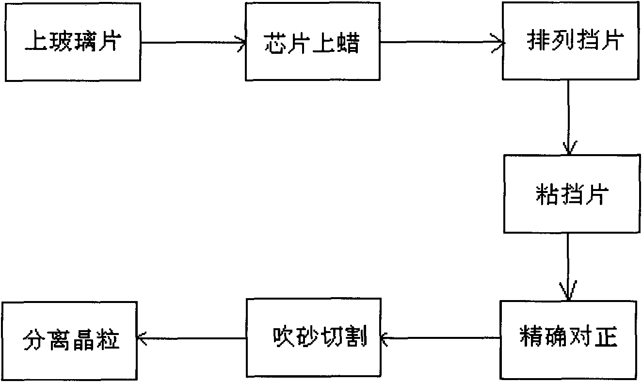
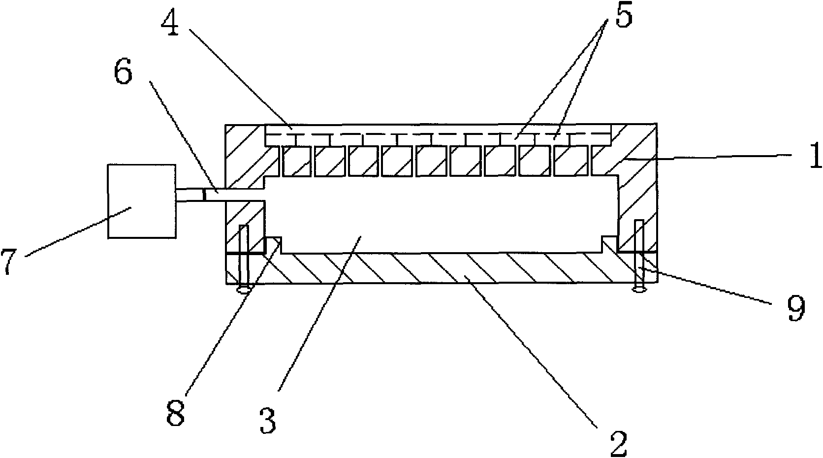
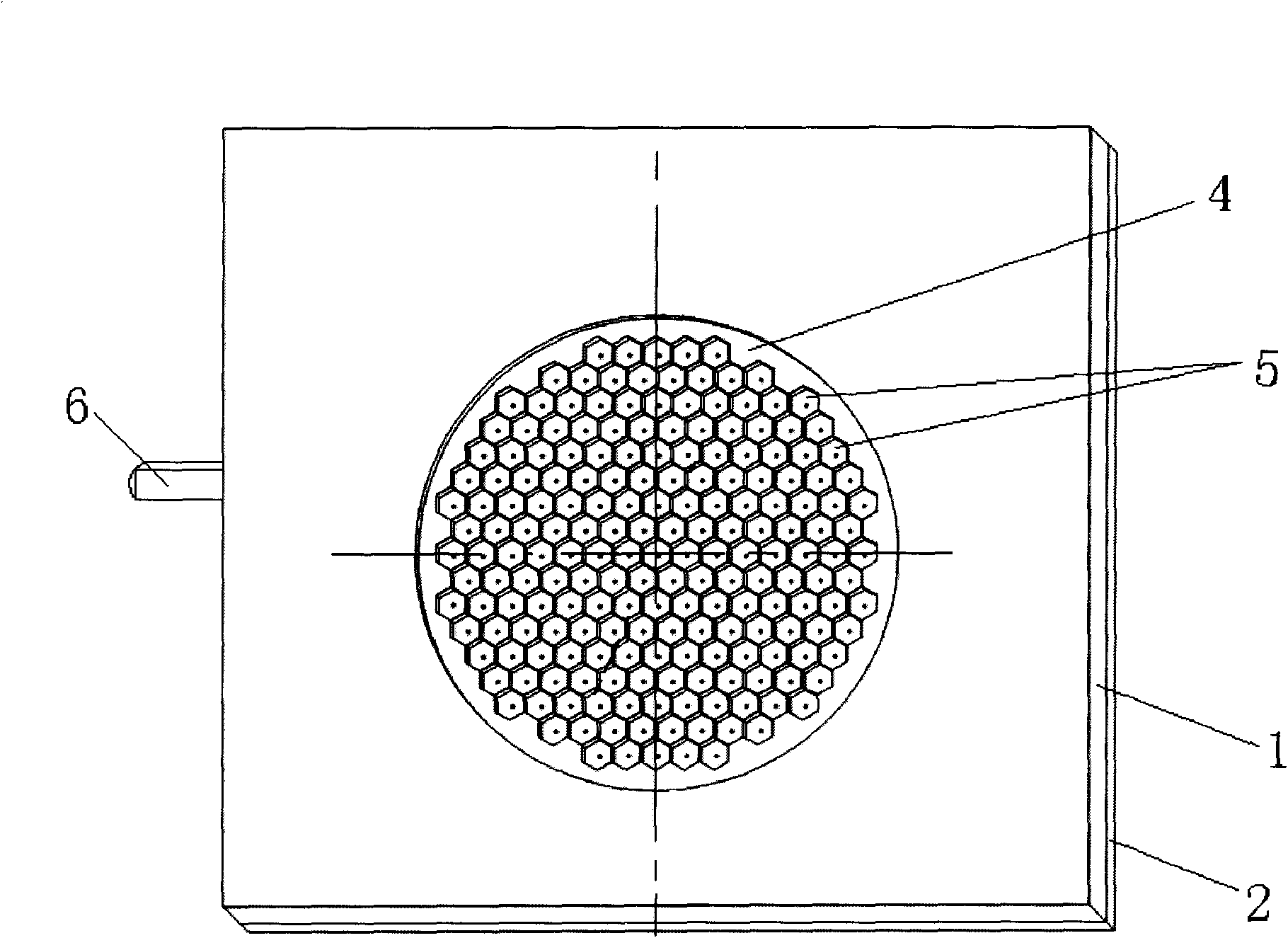
[0029] Such as figure 1 A method for producing rectifier crystal grains is shown, which includes firstly applying photoresist on the diffused silicon chip. The process is as follows: on the vacuum rotary machine, the terminal sucks the chip, drops a few drops of photoresist and rotates until uniform, and bakes. Dry; repeat the reverse side once, so that there is photoresist on both sides, and dry. Prepare two identical MASK films with graphic lines printed on them. The pattern formed by the graphic lines is a plurality of regular hexagons closely arranged in a honeycomb shape. Under the microscope, paste the MASK film on both sides of the silicon chip respectively, and align the patterns of the MASK film on both sides, expose and fix the silicon chip placed in the middle of the two MASK films at the same time, and then follow the fixed pattern on both sides of the silicon chip. Groove the pattern line, first open a shallow groove on the back of the silicon chip, apply photore...
PUM
 Abstract
Description
Claims
Application Information