Method and device for realizing communication between central processing unit and function chip

A central processing unit and functional technology, applied in the field of communication, can solve problems such as limited scale, low work efficiency, complex system, etc., and achieve the effect of expanding management scope, increasing work speed and reducing complexity

Inactive Publication Date: 2017-05-31
北京格林伟迪科技股份有限公司 +2
View PDF5 Cites 3 Cited by
  • Summary
  • Abstract
  • Description
  • Claims
  • Application Information

AI Technical Summary

Problems solved by technology

[0005] In view of this, the present application provides a method and device for realizing the communication between the central processing unit and the functional chip, so as to solve the problems of complex system, limited scale and low work efficiency

Method used


Image

  • Method and device for realizing communication between central processing unit and function chip
  • Method and device for realizing communication between central processing unit and function chip
  • Method and device for realizing communication between central processing unit and function chip

Examples


Embodiment Construction

[0023] In order to make the object, technical solution and advantages of the present invention clearer, the technical solution of the present invention will be described in detail below with reference to the accompanying drawings and examples.

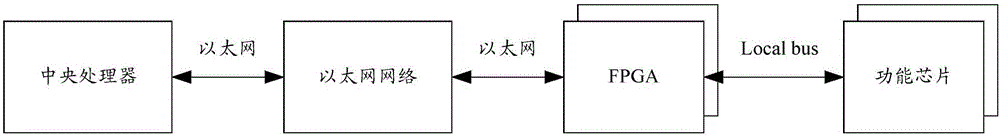
[0024] In a complex system, many chips with various functions are required to coordinate and realize the overall function of the system. For this reason, the central processing unit is required to manage and control each function chip.

[0025] When the system was relatively large, it was difficult for the central processing unit to directly receive each functional chip through the local bus. When the application was implemented in detail, a field programmable gate array (FPGA, Field Programmable Gate Array), the FPGA communicates with the central processing unit through Ethernet, and communicates with each functional chip through a local bus.

[0026] see figure 1 , figure 1 It is a schematic diagram of the system structure in the e...


PUM


Abstract

The invention provides a method and device for realizing communication between a central processing unit and a function chip. The method comprises the steps of when an FPGA (Field Programmable Gate Array) receives a command Ethernet frame sent by the central processing unit, carrying out caching; when a complete command Ethernet frame is cached, reading an operation command in the command Ethernet frame from a cache and generating a signal and a time sequence corresponding to the function chip for operation on a local bus according to the operation command; reading data from the local bus and storing the data; and when the operation command in the complete command Ethernet frame is finished, generating a return Ethernet frame for returning a performance result through utilization of stored data and the operation command according to a pre-defined frame structure, and sending the return Ethernet frame to the central processing unit. According to the technical scheme, a management range of the central processing unit can be expanded, the system complexity is reduced, and a working rate of the central processing unit is improved.

Description

technical field [0001] The invention relates to the technical field of communication, in particular to a method and a device for realizing communication between a central processing unit and a functional chip. Background technique [0002] In a complex communication device, it often consists of a main control board and multiple tributary boards with various functions, and each board has multiple chips to realize various functions. [0003] Generally, the processor on the main control board is connected to each chip through the local bus (local bus) to perform functions such as control, status reporting, or other information transmission to achieve coordinated work. However, this method has certain limitations. If more The connection is long, and the rate is limited due to the long line, which reduces the working speed of the processor; the long line distance will also lead to stability and prone to problems; direct management with a large span cannot be achieved, and the sys...

Claims


Application Information

Patent Timeline
Patent Type & Authority Applications(China)
IPC IPC(8): H04L12/40H04L1/00
Inventor 高卫东盖鹏飞陈磊
Owner 北京格林伟迪科技股份有限公司
Why Eureka
Try Eureka