Splicing structure of printed circuit board and splicing method

A technology for printed circuit boards and splicing surfaces, which is applied in the structural connection of printed circuits, printed circuits, printed circuit components, etc., can solve the problems of increasing product scrap rate and complicated production process of printed circuit boards, and achieve the reduction of splicing costs, The effect of improving stitching quality

Pending Publication Date: 2017-05-31
SHANGHAI UNITECH ELECTRONICS CO LTD
View PDF6 Cites 4 Cited by
  • Summary
  • Abstract
  • Description
  • Claims
  • Application Information

AI Technical Summary

Problems solved by technology

[0002] When the printed circuit board is shipped to the customer, multiple printed circuit boards will be spliced ​​into a whole piece according to the customer's needs to form a printed circuit board splicing block, and then shipped, and the production process of the printed circuit board is relatively complicated. It is inevitable that there will be some scrapped products, an...

Method used


Image

  • Splicing structure of printed circuit board and splicing method
  • Splicing structure of printed circuit board and splicing method

Examples


Embodiment Construction

[0025] In order to make the technical means, creative features, goals and effects achieved by the present invention easy to understand, the present invention will be further described below in conjunction with specific illustrations.

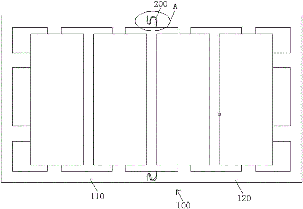
[0026] refer to figure 1 and figure 2 As shown in the figure, a splicing structure of a printed circuit board is shown in the figure, which includes a motherboard 110 and a daughter board 120 spliced ​​at one end of the motherboard 110 .

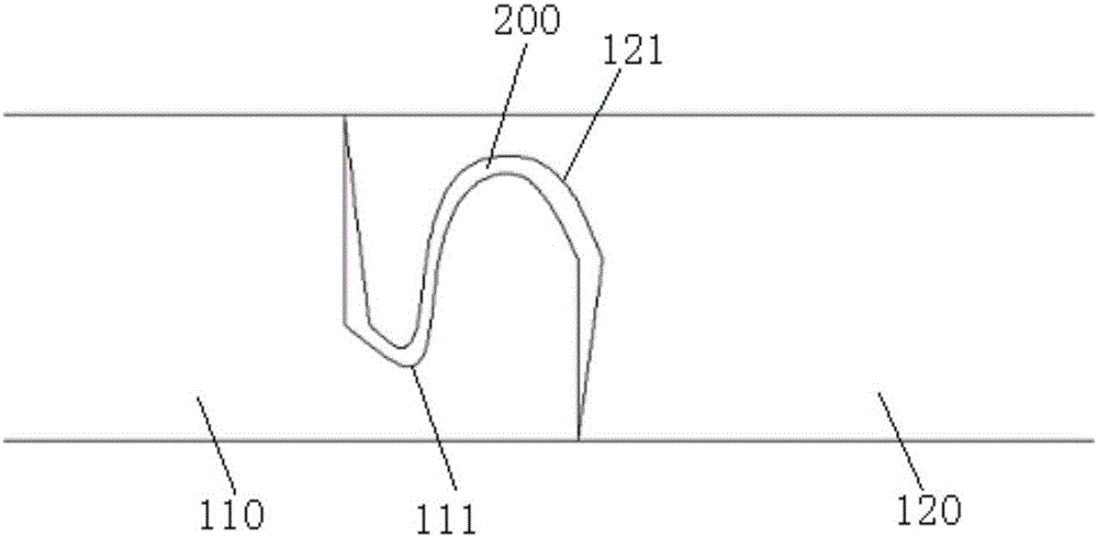
[0027] A motherboard splicing surface 111 is provided at the end where the motherboard 110 is spliced ​​with the daughterboard 120 , and a daughterboard splicing surface 121 is provided at the end where the daughterboard 120 is spliced ​​with the motherboard 110 .

[0028] The splicing surface 111 of the motherboard and the splicing surface 121 of the daughter board are spliced ​​to form a splicing structure 200. The two ends of the splicing structure 200 are butted and the middle part is provided with a cav...


PUM


Abstract

The invention discloses a splicing structure of a printed circuit board. The splicing structure includes a mother board and a child board spliced at one end of the mother board, the end, spliced with the child board, of the mother board is provided with a mother board splicing surface, the end, spliced with the mother board, of the child board is provided with a child board splicing surface, the mother board splicing surface is spliced with the child board splicing surface to form the splicing structure, the two ends of the splicing structure are in butt joint, and the middle of the splicing structure is provided with a cavity used for pouring thermocuring adhesives. The splicing structure of the printed circuit board not only can improve the splicing quality of the printed circuit board, but also can reduce the splicing cost and achieve environmental protection.

Description

technical field [0001] The invention relates to the technical field of splicing printed circuit boards, in particular to a splicing structure and splicing method of printed circuit boards. Background technique [0002] When the printed circuit board is shipped to the customer, multiple printed circuit boards will be spliced ​​into a whole piece according to the customer's needs to form a printed circuit board splicing block, and then shipped, and the production process of the printed circuit board is relatively complicated. It is inevitable that there will be some scrapped products, and the printed circuit board splicing blocks with scrapped products will be sent to the customer. The customer generally does not accept the scrapped products in the printed circuit board splicing block, so the scrapping of a single or multiple printed circuit board products will scrap the entire Printed circuit board splicing blocks, thereby increasing the scrap rate of the product. [0003] H...

Claims


Application Information

Patent Timeline
IPC IPC(8): H05K1/14H05K3/36
CPCH05K1/142H05K3/36H05K2203/17
Inventor 孙书勇徐兵
Owner SHANGHAI UNITECH ELECTRONICS CO LTD
Why Eureka
Try Eureka