Manufacture method of circuit board slot bottom graphics

A production method and circuit board technology, which is applied in multilayer circuit manufacturing, printed circuit manufacturing, printed circuit, etc., can solve problems such as unsuitable for large-scale production and application, design restrictions, and complicated protection methods, and achieve good production effects, Good matching effect

Active Publication Date: 2017-05-31
DONGGUAN SHENGYI ELECTRONICS
View PDF3 Cites 22 Cited by
  • Summary
  • Abstract
  • Description
  • Claims
  • Application Information

AI Technical Summary

Problems solved by technology

At present, there are various methods for manufacturing stepped groove circuit boards, but the biggest limitation for the large-scale application of stepped groove circuit boards is the production of line patterns at the bottom of the stepped grooves, especially the production of the bottom patterns of the stepped grooves with non-metallized side walls. Due to prefabricated groove bottom graphics, special methods are required to protect the graphics in the groove when making stepped grooves, especially when there are through holes at the bottom of the groove, the protection method is extremely complicated, and the precise production of outer graphics is limited, which has great restrictions on the design. Not suitable for large-scale production and application

Method used


Image

  • Manufacture method of circuit board slot bottom graphics
  • Manufacture method of circuit board slot bottom graphics
  • Manufacture method of circuit board slot bottom graphics

Examples


Embodiment Construction

[0019] In order to make the object, technical solution and advantages of the present invention clearer, the present invention will be further described in detail below in conjunction with the accompanying drawings and embodiments. It should be understood that the specific embodiments described here are only used to explain the present invention, not to limit the present invention.

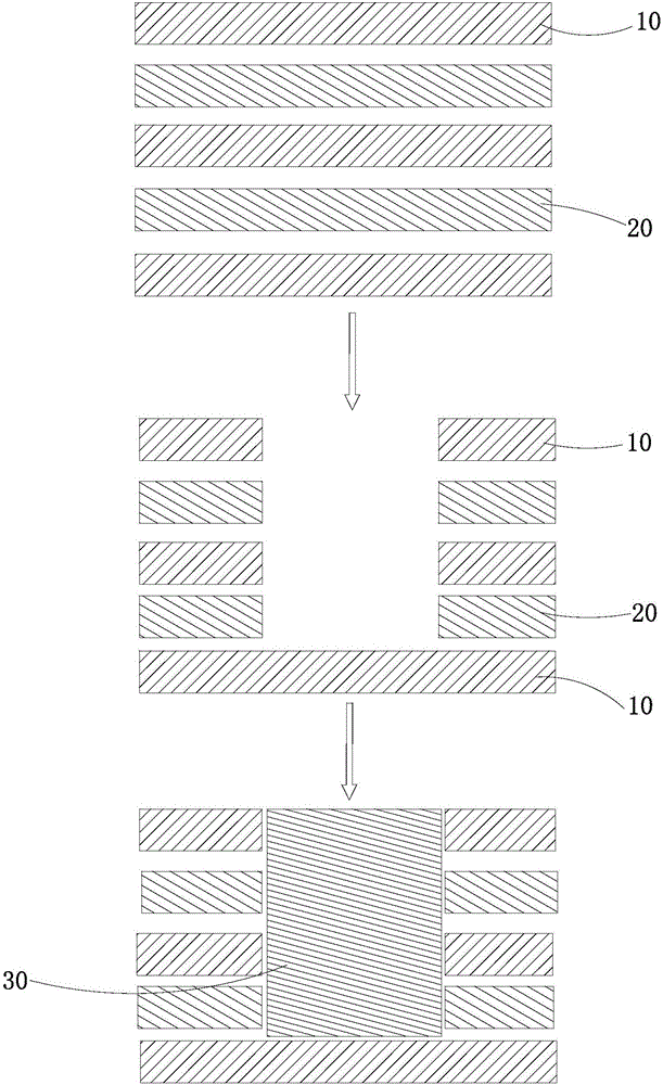
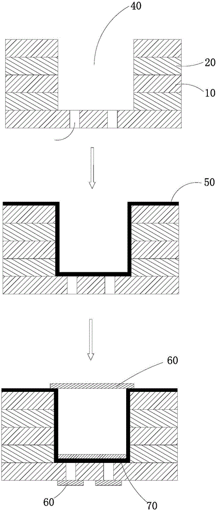
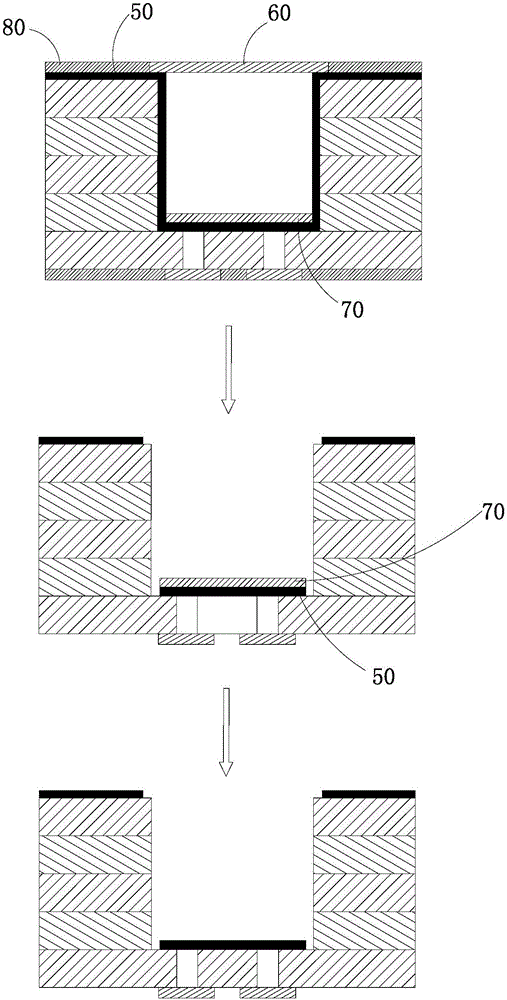
[0020] Such as Figure 1 to Figure 3 As shown, the present invention provides a kind of manufacturing method of circuit board groove bottom pattern, is used for PCB board groove bottom circuit pattern making, and it comprises the following steps:

[0021] Step (1), making core board graphics, preparing several core boards 10 and PP 20, each core board 10 includes an inner layer board and a copper layer attached to the upper and lower sides of the inner layer board, and opening the core board 10 and PP 20 After cutting the material, etch on the core board 10 to complete the pattern making;

[0022]...


PUM


Abstract

The invention discloses a manufacture method of circuit board slot bottom graphics. The method comprises the following steps: preparation before plate pressing, slotting, gasket laying, plate pressing and hole drilling, electroplating, adhesive tape adhering and dry film slot sealing treatment, electroplating of protection tin layer, etching of slot wall, adhesive tape tearing, and manufacture of graphics in slot. According to the method, a single side of the slot bottom is bonded through an antielectroplating adhesive tape after step slot electroplating, a protection drying film is manufactured, the opening of the step slot is completely sealed, then a protection tin layer is electroplated, etching is performed after stripping of the film, non metallization of the slot wall is realized, and graphics at the slot bottom are manufactured after the adhesive tape at the slot bottom is torn. The method is good in matching ability with the conventional flow, manufacture of exquisite graphics can be performed, meanwhile through holes can be manufactured in the slot bottom, special protection materials and special technical processes are not required, the method is suitable for large-scale manufacture, and the manufacture effect is good. No design limits exist for external layer graphics, and the method is suitable for batch manufacture of side wall non metallization step slot graphic panels.

Description

technical field [0001] The invention relates to a method for manufacturing a circuit board, in particular to a method for manufacturing a groove bottom pattern of a circuit board. Background technique [0002] Due to its special structure and electrical properties, the stepped groove has a wide range of applications in three-dimensional three-dimensional assembly, reducing the assembly volume of electrical equipment, and special electrical properties. At present, there are various methods for manufacturing stepped groove circuit boards, but the biggest limitation for the large-scale application of stepped groove circuit boards is the production of line patterns at the bottom of the stepped grooves, especially the production of the bottom patterns of the stepped grooves with non-metallized side walls. Due to prefabricated groove bottom graphics, special methods are required to protect the graphics in the groove when making stepped grooves, especially when there are through ho...

Claims


Application Information

Patent Timeline
Patent Type & Authority Applications(China)
IPC IPC(8): H05K3/46
CPCH05K3/4697H05K2203/0214
Inventor 焦其正王小平纪成光王洪府
Owner DONGGUAN SHENGYI ELECTRONICS
Why Eureka
Try Eureka