Method and system for extracting parasitic capacitance

A parasitic capacitance, integrated circuit technology, applied in the field of extracting parasitic capacitance, can solve the problems of geometric pattern deviation, inaccurate extraction of parasitic capacitance, etc., and achieve the effect of improving accuracy

Active Publication Date: 2017-06-09
INST OF MICROELECTRONICS CHINESE ACAD OF SCI
View PDF4 Cites 4 Cited by
  • Summary
  • Abstract
  • Description
  • Claims
  • Application Information

AI Technical Summary

Problems solved by technology

[0005] The present invention provides a method and system for extracting parasitic capacitance, which solves the problem of inaccurate extraction of parasitic capacitance caused by the geometric deviation between actual manufacturing and integrated circuit design in the integrated circuit manufacturing process,

Method used


Image

  • Method and system for extracting parasitic capacitance
  • Method and system for extracting parasitic capacitance
  • Method and system for extracting parasitic capacitance

Examples


Embodiment Construction

[0060] In order to enable those skilled in the art to better understand the solutions of the embodiments of the present invention, the embodiments of the present invention will be further described in detail below in conjunction with the drawings and implementations.

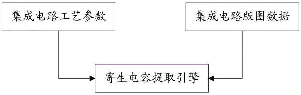
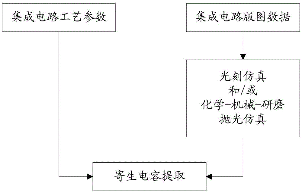
[0061] In the integrated circuit manufacturing process under the advanced integrated circuit technology, there is a deviation between the geometric figures actually manufactured and the geometric figures in the layout data obtained by design, which directly affects the accuracy of extracting parasitic capacitance and may cause the performance of circuit optimization The result is inaccurate.

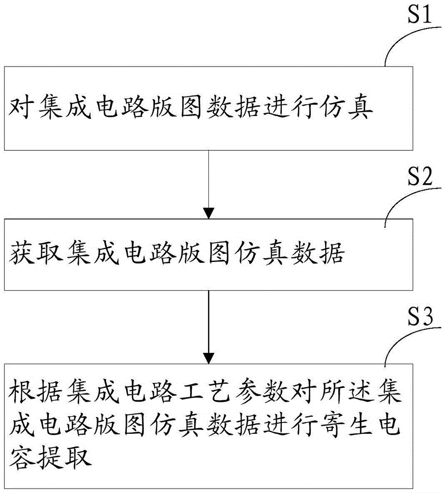
[0062] Such as figure 2 As shown, it is a flow chart of a method for extracting parasitic capacitance provided by the present invention. Include the following steps:

[0063] S1: Simulate the layout data of the integrated circuit;

[0064] S2: Acquiring integrated circuit layout simulation data;

[0065] S3: Perform p...


PUM


Abstract

The invention provides a method for extracting a parasitic capacitance. The method comprises the steps that integral circuit layout data is simulated; simulation data of integral circuit layout is acquired; and according to integral circuit technological parameters, the parasitic capacitance can be extracted from the integral circuit layout simulation data. The invention also provides a system for extracting the parasitic capacitance. According to the scheme provided by the invention, the problem that parasitic capacitance extraction is inaccurate due to geometric graph deflections of actual manufacture and integral circuit design during integral circuit manufacture can be solved effectively; and accuracy of the parasitic capacitance extraction can be increased.

Description

technical field [0001] The invention belongs to the field of integrated circuit design, and in particular relates to a method and system for extracting parasitic capacitance. Background technique [0002] With the development of technology, circuit optimization design has become an important stage in the integrated circuit design process. The purpose of circuit optimization is to improve the electrical performance of the circuit, and the final actual electrical performance of the circuit not only depends on the device parameter values ​​of the circuit, but also depends on the parasitic effect of the device itself, the parasitic effect between devices, the parasitic effect of the connection itself, the connection The parasitic effect between the lines, and the parasitic effect between the wiring and the device, and the parasitic effect between the adjacent wiring is particularly critical. From the perspective of circuit optimization theory, in order to obtain accurate circui...

Claims


Application Information

Patent Timeline
Patent Type & Authority Applications(China)
IPC IPC(8): G06F17/50
CPCG06F30/398
Inventor 吴玉平陈岚
Owner INST OF MICROELECTRONICS CHINESE ACAD OF SCI
Why Eureka
Try Eureka