Touch substrate, manufacturing method thereof and touch display device

A substrate and touch technology, applied in the fields of display and touch, can solve the problem of uneven distribution of capacitance in the touch area, improve touch accuracy and user experience, reduce internal mutual capacitance, and improve the uneven distribution of edge capacitance. Effect

Active Publication Date: 2017-06-13
BOE TECH GRP CO LTD +1
View PDF3 Cites 14 Cited by
  • Summary
  • Abstract
  • Description
  • Claims
  • Application Information

AI Technical Summary

Problems solved by technology

[0005] Aiming at the above problems in the prior art, the present invention provides a touch substrate and a manufacturing method thereof, which are used to at least partially improve the problem of uneven capacitance distribution in the touch area of ​​the existing touch substrate

Method used


Image

  • Touch substrate, manufacturing method thereof and touch display device
  • Touch substrate, manufacturing method thereof and touch display device
  • Touch substrate, manufacturing method thereof and touch display device

Examples


no. 1 example

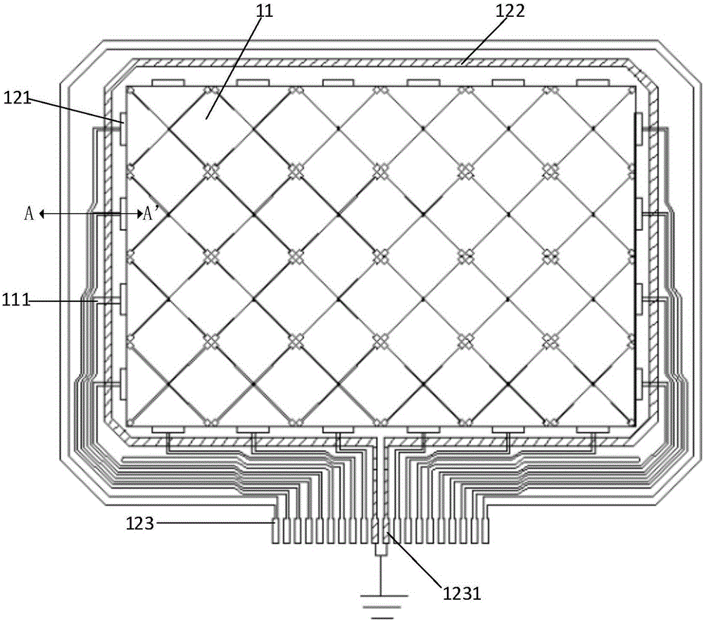
[0072] exist figure 1 , figure 2 and image 3 A first embodiment of the invention is shown.

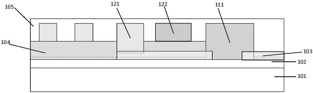
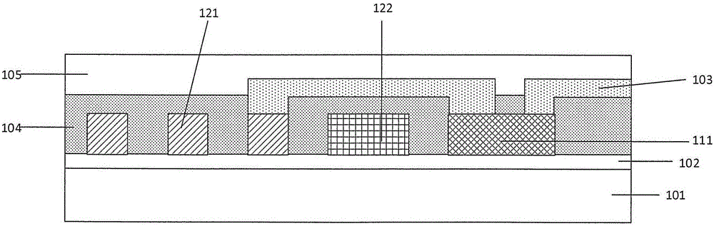
[0073] figure 1 is a schematic plan view of the touch substrate according to the first embodiment of the present invention, figure 2 is the substrate edge according to the first embodiment of the present invention figure 1 The schematic diagram of the cross-section in the direction of A-A', image 3 is another substrate edge according to the first embodiment of the present invention figure 1 The schematic diagram of the cross-section in the direction of A-A' is now combined with figure 1 , figure 2 and image 3 A first embodiment of the present invention will be described.

[0074] like figure 1 and figure 2 As shown, a specific embodiment of the present invention provides a touch substrate, including a substrate 1 . The substrate 1 is provided with a touch area 11 and a peripheral area 12 around the display area. The peripheral area 12 includes at least one signal tr...

no. 2 example

[0088] like Figure 4 and Figure 5 Shown is the second embodiment of the present invention.

[0089] Figure 4 is a schematic plan view of the touch substrate according to the second embodiment of the present invention, Figure 5 It is a partial enlarged perspective view of the touch substrate in the second embodiment of the present invention where the signal trace 121 and the metal bonding block 111 overlap.

[0090] like Figure 4 and Figure 5 As shown, a specific embodiment of the present invention provides a touch substrate, including a substrate 1 . The substrate 1 is provided with a touch area 11 and a peripheral area 12 around the display area. The peripheral area 12 includes at least one signal trace 121 and a shielding wire 122 . The touch control substrate further includes a peripheral grounding device or grounding line 13 located on the periphery of the signal line 121 . A peripheral grounding device or grounding wire 13 is electrically connected to the sh...

no. 3 example

[0104] like Image 6 or Figure 7 As shown, the embodiment of the present invention provides a manufacturing method of a touch substrate, the manufacturing method comprising:

[0105] like Image 6 As shown, a touch area and a peripheral area are set on the touch substrate. Make a black matrix on the substrate, the structure of the black matrix is ​​as follows figure 2 The middle black matrix 102 is used to form a light-shielding area.

[0106] An ITO layer is formed on the black matrix, and an ITO pattern is formed through a patterning process. The ITO pattern includes an ITO bridge for connecting signal lines and metal bonding blocks. The ITO bridge structure is as follows Figure 5 Middle ITO Bridge 1031.

[0107] A first insulating layer is formed on the ITO layer, and the first insulating layer has a structure such as figure 2 The middle first insulating layer 104 . Make a via hole on the first insulating layer, the via hole structure is as Figure 5 The via hol...


PUM


Abstract

The invention discloses a touch substrate, a manufacturing method thereof and a touch display device and belongs to the technical field of touch control. The touch substrate comprises a touch area and a peripheral area which are located on the substrate. The peripheral area comprises at least one signal line and at least one shielding line, and the shielding line is used for shielding interference of the signal line on the capacitance of the touch area. By means of the touch substrate, interference of the signal line on the touch area can be shielded, and the problem that the capacitance of a touch substrate is not uniform in distribution is alleviated.

Description

technical field [0001] The present invention relates to the field of display and touch technology, in particular to a touch substrate, a manufacturing method thereof, and a touch display device. Background technique [0002] With the rapid development of smart phones and tablet computers, touch screens have been widely used in daily life. At present, the most popular is the capacitive touch screen. When the finger touches the screen, the touch screen will calculate the position of the finger through the current generated by the capacitance change. [0003] Generally, a touch substrate includes a touch area and a peripheral area. Among them, the touch area is the area where the user can see the image and touch it, and the peripheral area includes a plurality of signal lines for providing control signals for the touch area, that is, one end of the signal line is connected to the touch area, and the other end Connect various drive control signals. [0004] With the developme...

Claims


Application Information

Patent Timeline
Patent Type & Authority Applications(China)
IPC IPC(8): G06F3/044G06F3/041
CPCG06F3/0412G06F3/044G06F3/04164G06F2203/04107G06F3/0443G06F3/0446G06F2203/04103
Inventor 范文金张雷郭总杰张志贺晓悦
Owner BOE TECH GRP CO LTD
Why Eureka
Try Eureka