

Method of Optimizing PCB Microstrip Line Structure Based on Response Surface Method and Genetic Algorithm
A technology of response surface method and genetic algorithm, applied in the field of signal integrity of microelectronic packaging, can solve problems such as noise and interference of transmission signals, and achieve the effects of simple calculation, excellent robust performance, and convenient parameter optimization design.
- Summary
- Abstract
- Description
- Claims
- Application Information
AI Technical Summary
Problems solved by technology
Method used
Image

Examples
Embodiment
[0040] The method for optimizing the PCB microstrip line structure based on the response surface method and the genetic algorithm specifically includes the following steps:
[0041] (1) Establish the microstrip line simulation analysis model of HFSS, and the model substrate size is shown in Table 1;
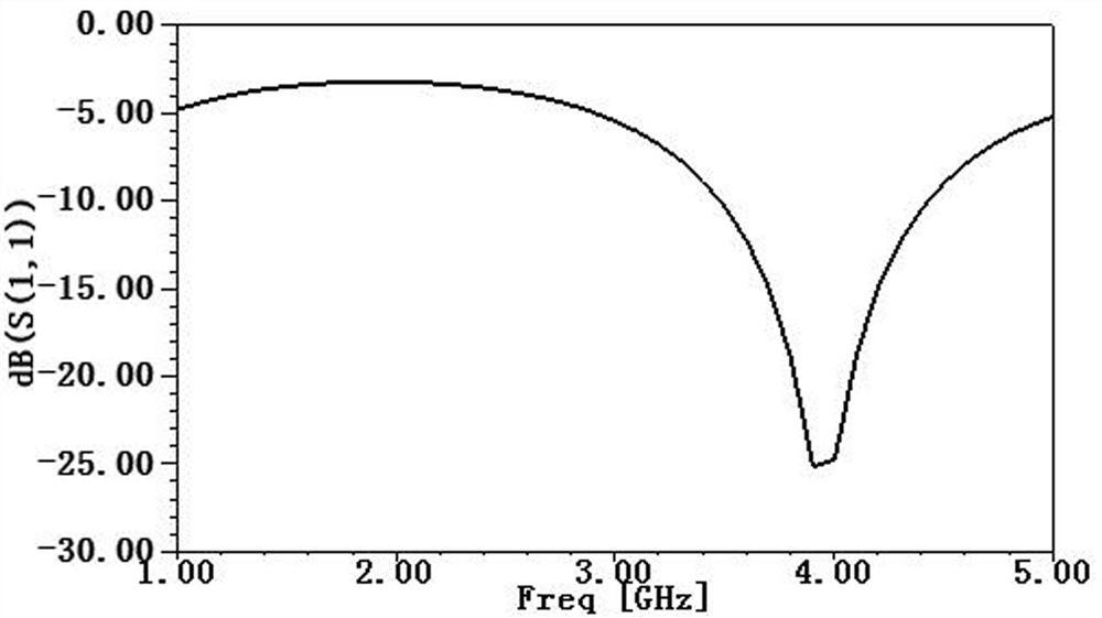
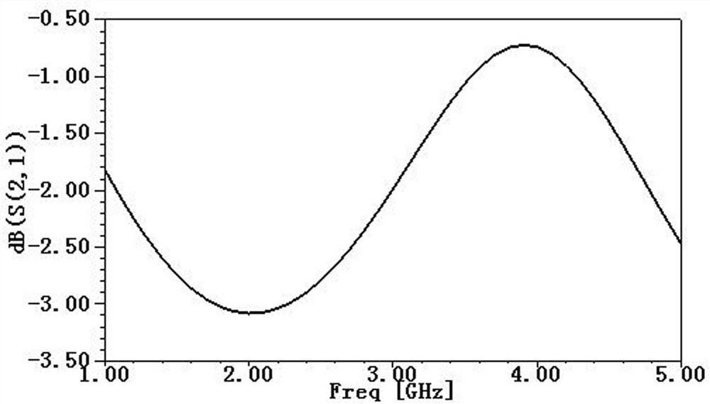
[0042] (2) Obtain the return loss S11 and insertion loss S21 at a frequency of 1GHz-5GHz, such as figure 1 , 2 shown;
[0043] (3) Obtain the influencing factors affecting the microstrip line as follows: substrate thickness H1, microstrip line width t, microstrip line thickness H2, and substrate dielectric constant E; select three levels for each factor respectively, and the factor levels are as follows As shown in Table 2;
[0044] (4) Using BOX-Behnken's central combination design model, there are 29 groups of simulation model level combinations, of which 24 groups are analysis factors, and 5 groups are zero-point factors, that is, the parameter level combinations are the sa...
PUM
 Abstract
Description
Claims
Application Information