Sound wave type fingerprint recognizing device, manufacturing method thereof and electronic device using same

A fingerprint recognition and sound wave technology, applied in the field of sound wave fingerprint recognition devices, can solve problems such as adverse effects of sensing, achieve the effects of saving materials and processes, accurate sensing results, and reducing noise

Active Publication Date: 2017-06-20
INTERFACE TECH CHENGDU CO LTD +1
View PDF6 Cites 6 Cited by
  • Summary
  • Abstract
  • Description
  • Claims
  • Application Information

AI Technical Summary

Problems solved by technology

[0005] In view of this, the present invention provides an acoustic wave fingerprint identification device, which effectively solves the problem of adv

Method used


Image

  • Sound wave type fingerprint recognizing device, manufacturing method thereof and electronic device using same
  • Sound wave type fingerprint recognizing device, manufacturing method thereof and electronic device using same
  • Sound wave type fingerprint recognizing device, manufacturing method thereof and electronic device using same

Examples


no. 1 example

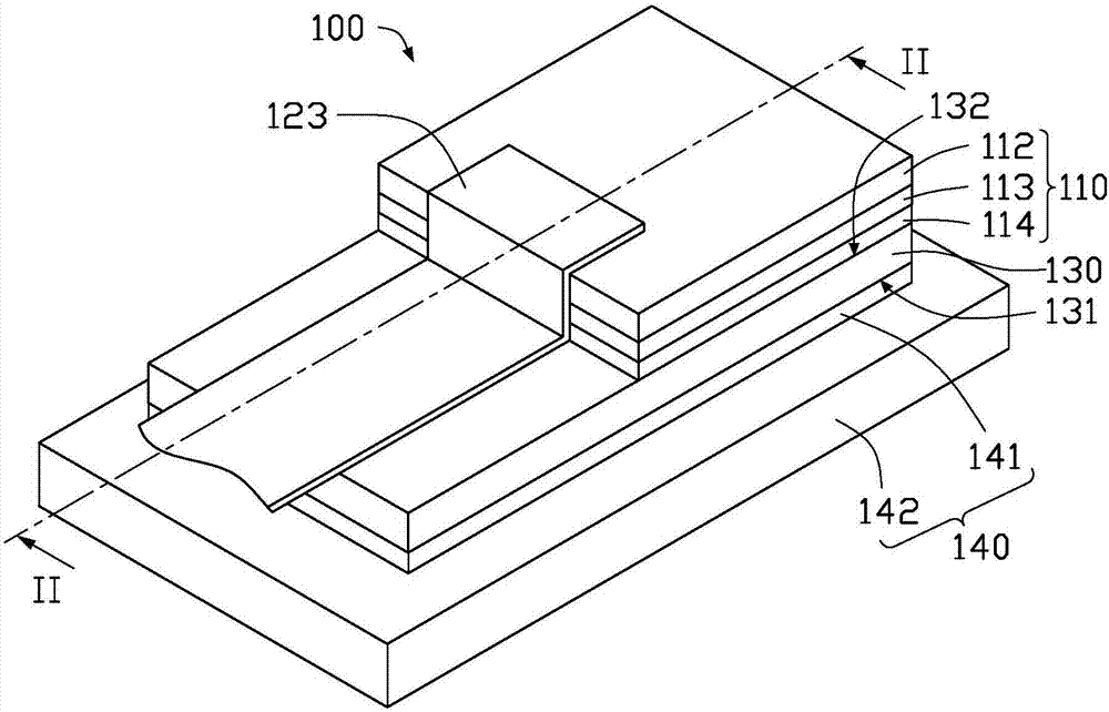
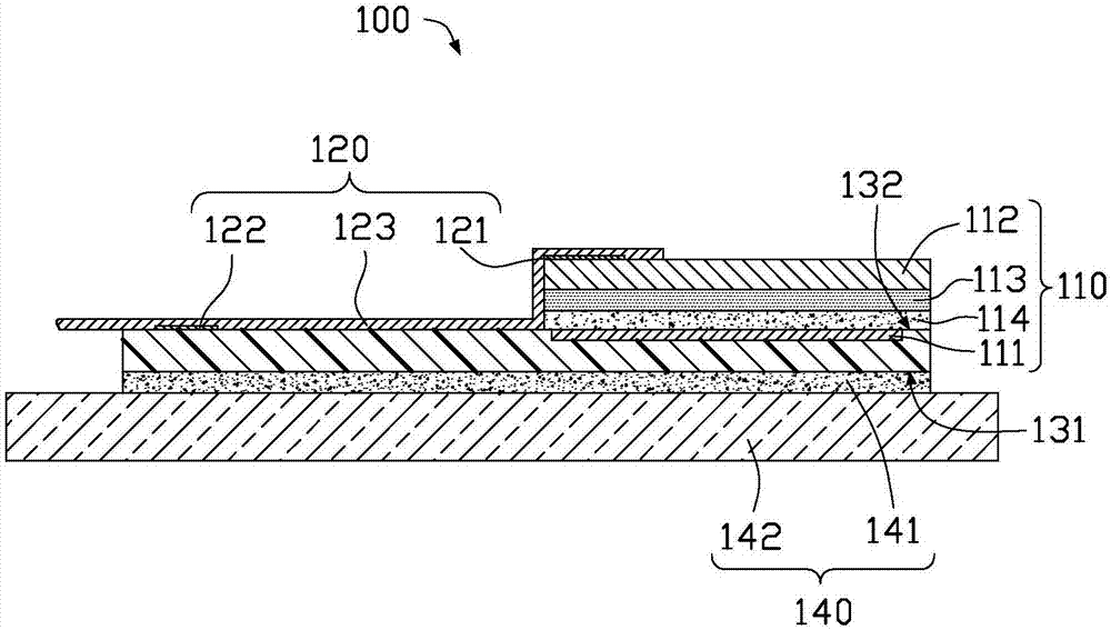
[0037] Such as figure 1 and figure 2 As shown, the acoustic wave fingerprint identification device 100 according to the first embodiment of the present invention includes a cover plate 140 , a circuit substrate 130 , a signal transmission unit 120 , and an ultrasonic sensing unit 110 .

[0038] The circuit substrate 130 is fixed on one side of the cover plate 140, the ultrasonic sensing unit 110 is arranged on the side of the circuit substrate 130 away from the cover plate 140, one end of the signal transmission unit 120 is connected to a control device (not shown), and the other end is simultaneously connected to The ultrasonic sensing unit 110 and the circuit substrate 130 are used to realize signal transmission between the control device and the ultrasonic sensing unit 110 and the circuit substrate 130 .

[0039] The cover plate 140 includes a cover glass 142 and a first adhesive layer 141 , and the cover glass 142 is combined with the circuit substrate 130 through the fi...

no. 2 example

[0057] Such as Figure 4 and Figure 5 As shown, the acoustic wave fingerprint identification device 200 according to the second embodiment of the present invention includes a cover plate 240 , a circuit substrate 230 , an ultrasonic sensing unit 210 , and a signal transmission unit 220 .

[0058] The circuit substrate 230 is fixed on one side of the cover plate 240, the ultrasonic sensing unit 210 is arranged on the side of the circuit substrate 230 away from the cover plate 240, one end of the signal transmission unit 220 is connected to a control device (not shown), and the other end is simultaneously connected to The ultrasonic sensing unit 210 and the circuit substrate 230 are used to realize signal transmission between the control device and the ultrasonic sensing unit 210 and the circuit substrate 230 .

[0059] The cover plate 240 includes a cover glass 242 and a first adhesive layer 241 , and the cover glass 242 is combined with the circuit substrate 230 through the ...


PUM

PropertyMeasurementUnit
Thicknessaaaaaaaaaa
Resistivityaaaaaaaaaa

Abstract

The invention provides a sound wave type fingerprint recognizing device which comprises a circuit board, an ultrasonic sensing unit and a signal transmission unit, wherein the ultrasonic sensing unit and the signal transmission unit are formed on the surface of the circuit board. The circuit board comprises a circuit. The ultrasonic sensing unit comprises a surface arranged on the circuit board, a first electrode, a piezoelectric polymer layer and a second electrode, wherein the first electrode, the piezoelectric polymer layer and the second electrode are electrically connected with the circuit. The signal transmission unit is electrically connected with the circuit and the second electrode to realize signal transmission. The second electrode directly contacts the piezoelectric polymer layer. The second electrode is the outer protective structure of the ultrasonic sensing unit. The invention further provides a manufacturing method of the sound wave type fingerprint recognizing device and an electronic device which uses the sound wave type fingerprint recognizing device.

Description

technical field [0001] The invention relates to an acoustic wave fingerprint identification device, a manufacturing method thereof and an electronic device using the acoustic wave fingerprint identification device. Background technique [0002] With the widespread use of portable electronic devices, users have put forward more functional requirements for portable electronic devices. Due to the privacy protection function, the fingerprint identification device is installed in the portable electronic device to enhance user experience. Fingerprint identification devices can be divided into optical, capacitive, and acoustic wave types. Acoustic fingerprint identification devices are widely used because their operations are not easily affected by ambient temperature and humidity, and they have a long life and high resolution. [0003] The ultrasonic fingerprint identification element can identify the fingerprint of a finger placed on the fingerprint identification element. Whe...

Claims


Application Information

Patent Timeline
IPC IPC(8): G06K9/00
CPCG06V40/13
Inventor 郑小兵
Owner INTERFACE TECH CHENGDU CO LTD
Why Eureka
Try Eureka