Broken wire repair method for array substrate

A technology of array substrates and substrate substrates, applied in nonlinear optics, instruments, optics, etc., can solve problems such as LCVD long line breakage

Inactive Publication Date: 2017-06-27
SHENZHEN CHINA STAR OPTOELECTRONICS TECH CO LTD
View PDF6 Cites 5 Cited by
  • Summary
  • Abstract
  • Description
  • Claims
  • Application Information

AI Technical Summary

Problems solved by technology

[0004] The present invention provides a method for repairing disconnection of an array substrate, which is used to so...

Method used


Image

  • Broken wire repair method for array substrate
  • Broken wire repair method for array substrate
  • Broken wire repair method for array substrate

Examples


Embodiment Construction

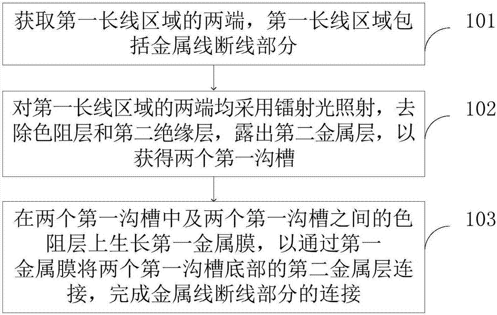
[0032] The present invention will be further described below in conjunction with accompanying drawing.

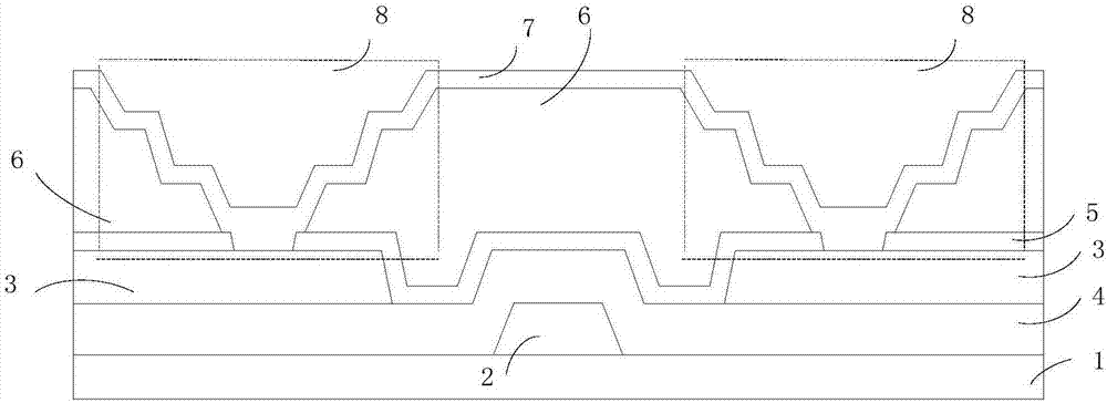
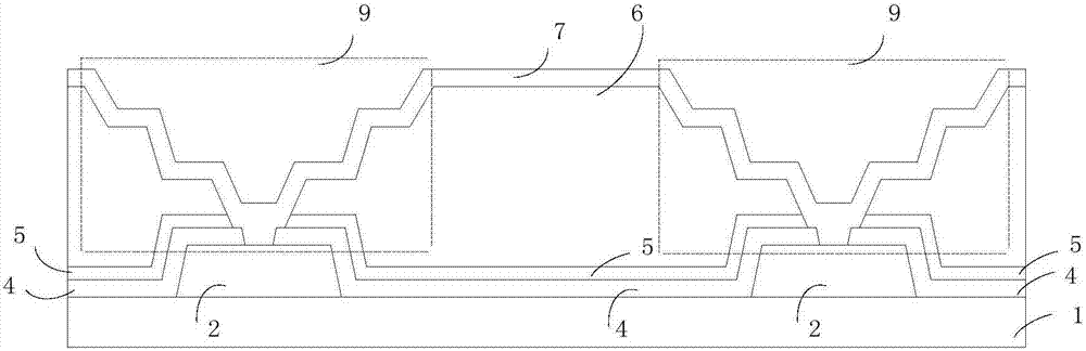
[0033] Please refer to figure 1 and figure 2 . This embodiment provides a method for repairing disconnection of an array substrate. The array substrate includes a base substrate 1, a first metal layer 2, a second metal layer 3, a first insulating layer 4, a second insulating layer 5, and a color resist layer 6; Wherein, the first metal layer 2 is disposed on the base substrate 1, the first insulating layer 4 covers the first metal layer 2 and the base substrate 1, the second metal layer 3 is located on the first insulating layer 4, and the second insulating layer 4 covers the first metal layer 2 and the base substrate 1. The layer 5 covers the second metal layer 3 and the first insulating layer 4, and the color resistance layer 6 covers the second insulating layer 5, including:

[0034] In step 101, two ends of a first long-line area are obtained, and the first long-lin...


PUM


Abstract

The invention provides a broken wire repair method for an array substrate. The method includes the steps that the two ends of a first long wire region are acquired, wherein the first long wire region comprises a metal wire broken wire part; the two ends of the first long wire region are subjected to laser light irradiation, a color resistance layer and a second insulating layer are removed, a second metal layer is exposed, two first grooves are obtained, and the side walls of the first grooves are in step shapes; first metal films grow in the two first grooves and on the color resistance layer between the two first grooves, second metal layers at the bottoms of the two first grooves are connected through the first metal films, and connection of the metal wire broken wire part is completed. Due to the fact that the side walls of the first grooves obtained through the method are in the step shapes, in other words, the descending process of the side walls of the first grooves formed in the color resistance layer and the second insulating layer is slow, the climbing height of the first metal films is greatly reduced, the first metal films are not prone to breakage, and the success rate of broken wire repair is increased.

Description

technical field [0001] The present invention relates to the field of display technology, in particular to a method for repairing disconnection of an array substrate. Background technique [0002] With the continuous development of liquid crystal panel technology, more and more new technologies are applied to thin film transistor array substrates, such as in-plane switching (In-Plane Switching, referred to as IPS), fringe field switching technology (Fringe Field Switching, referred to as FFS), color Filter matrix (Color Filter On Array, referred to as COA) and other technologies. These technologies have relatively high requirements on the flatness of the display substrate, and usually need to deposit a thick organic layer such as a color resist layer and a flat layer on the array substrate. During the fabrication process of the array substrate, due to the influence of various factors, metal wires including scan lines and data lines may be disconnected or short-circuited, whi...

Claims


Application Information

Patent Timeline
IPC IPC(8): G02F1/1362
CPCG02F1/136259G02F1/136263
Inventor 胡建平谢克成
Owner SHENZHEN CHINA STAR OPTOELECTRONICS TECH CO LTD
Why Eureka
Try Eureka