

A linear transconductance conversion circuit system
Patent Information
- Authority / Receiving Office
- CN · China
- Patent Type
- Patents(China)
- Current Assignee / Owner
- GUANGZHOU INTELLIGENT CITY DEV INST
- Publication Date
- 2019-01-29
Smart Images
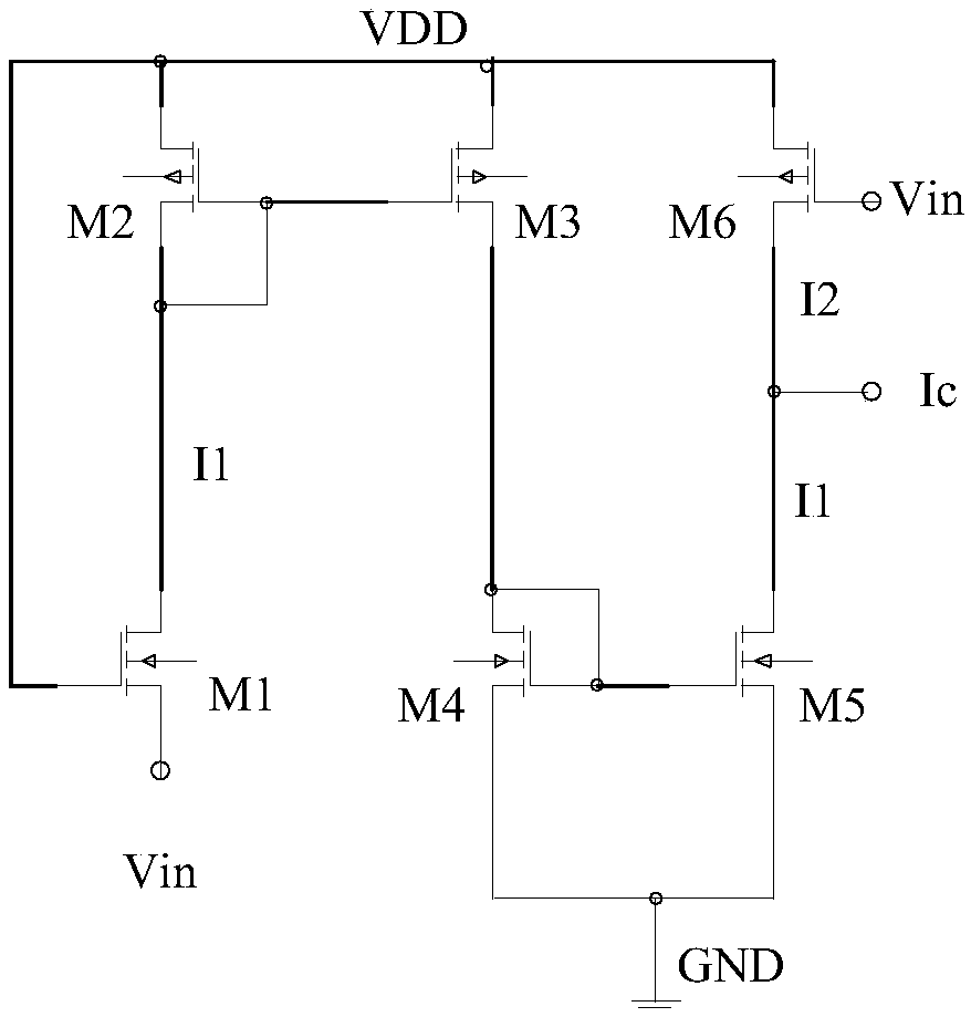
Figure 1 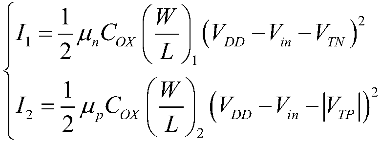
Figure 2 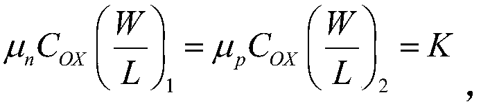
Figure 3
Abstract
Description
technical field
[0001] The invention relates to the technical field of chip transconductance conversion circuits, in particular to a linear transconductance conversion circuit system. Background technique
[0002] A variable gain amplifier (variable gain amplifier, VGA) has a wide range of applications in systems that need to process analog signals, such as hearing aids, hard disks, and communications. The core circuit of VGA is the current square circuit. The output current of this circuit has a square relationship with the input current, but the input and output in VGA are voltage signals, so it is necessary to linearly convert the input voltage signal into a current signal, and then send it to Into the current square circuit, and finally the output current signal is linearly converted into a voltage signal. Contents of the invention
[0003] The object of the present invention is to overcome the deficiencies in the prior art. The present invention provides a linear tra...