Supercharge Your Innovation With Domain-Expert AI Agents!

Multi-region power semiconductor devices

A region and gate region technology used in the field of power semiconductor devices

Active Publication Date: 2021-08-31
FORD GLOBAL TECH LLC
View PDF5 Cites 0 Cited by
  • Summary
  • Abstract
  • Description
  • Claims
  • Application Information

AI Technical Summary

Problems solved by technology

For a given technical performance, existing designs cannot achieve low-loss on-state and low-loss switching behavior of switching transistors within the same chip

Method used


Image

  • Multi-region power semiconductor devices
  • Multi-region power semiconductor devices
  • Multi-region power semiconductor devices

Examples


Embodiment Construction

[0019] As required, detailed embodiments of the present invention are disclosed herein; however, it is to be understood that the disclosed embodiments are merely exemplary of the invention, which may be embodied in various and alternative forms. The figures are not necessarily to scale; some features may be exaggerated or minimized to show details of particular components. Therefore, specific structural and functional details disclosed herein are not to be interpreted as limiting, but merely as a representative basis for teaching one skilled in the art to variously employ the present invention.

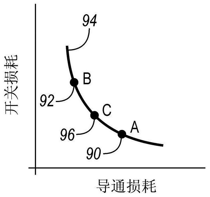
[0020] Power semiconductor devices (especially bipolar power semiconductor devices using minority carrier conduction) are designed according to the balance curve between conduction loss and switching loss. Products designed to enable high-frequency switching typically utilize relatively high on-state on-state voltages to optimize switching loss performance, and vice versa.

[0021] I...


PUM


Abstract

The invention discloses a multi-region power semiconductor device. A power semiconductor device is composed of a plurality of regions having similar structures. Each of the regions can be characterized by switching losses during switching to the non-conducting state. The device is configured such that switching losses differ between at least two of the regions. Furthermore, the device is configured such that regions with greater switching losses are switched into a non-conducting state before regions with smaller switching losses.

Description

technical field [0001] The present application relates generally to power semiconductor devices. Background technique [0002] Power semiconductor devices (especially bipolar power semiconductor devices using minority carrier conduction) are designed according to the trade-off curve between conduction loss and switching loss. Products designed to enable high frequency switching typically utilize relatively high on-state on-state voltages to optimize switching loss performance. Products designed for low-frequency switching typically take advantage of relatively high switching losses to optimize conduction loss performance. For a given technical performance, existing designs do not enable switching transistors to achieve low-loss on-state and low-loss switching behavior within the same chip. Contents of the invention [0003] In some configurations, an insulated gate bipolar transistor includes a first region and a second region, the first region and the second region each...

Claims


Application Information

Patent Timeline
Patent Type & Authority Patents(China)
IPC IPC(8): H01L29/739H01L29/06H01L29/08H01L29/10
CPCH01L29/0611H01L29/0684H01L29/0821H01L29/1004H01L29/7393H01L29/7395H01L27/0825H01L29/7397H01L29/0696H01L29/1095H01L27/082
Inventor 苏明
Owner FORD GLOBAL TECH LLC
Features
  • R&D
  • Intellectual Property
  • Life Sciences
  • Materials
  • Tech Scout
  • Unparalleled Data Quality
  • Higher Quality Content
  • 60% Fewer Hallucinations
Learn More