Method for analyzing fatigue life of electronic packaging welding spot

A fatigue life analysis, electronic packaging technology, used in electronic circuit testing, measuring electricity, measuring devices, etc.

Inactive Publication Date: 2017-07-07
UNIV OF ELECTRONICS SCI & TECH OF CHINA
View PDF6 Cites 22 Cited by
  • Summary
  • Abstract
  • Description
  • Claims
  • Application Information

AI Technical Summary

Problems solved by technology

However, there are few relevant studies on the uncertainty of various internal and external factors that affect the fatigue life of s

Method used


Image

  • Method for analyzing fatigue life of electronic packaging welding spot
  • Method for analyzing fatigue life of electronic packaging welding spot
  • Method for analyzing fatigue life of electronic packaging welding spot

Examples


Embodiment Construction

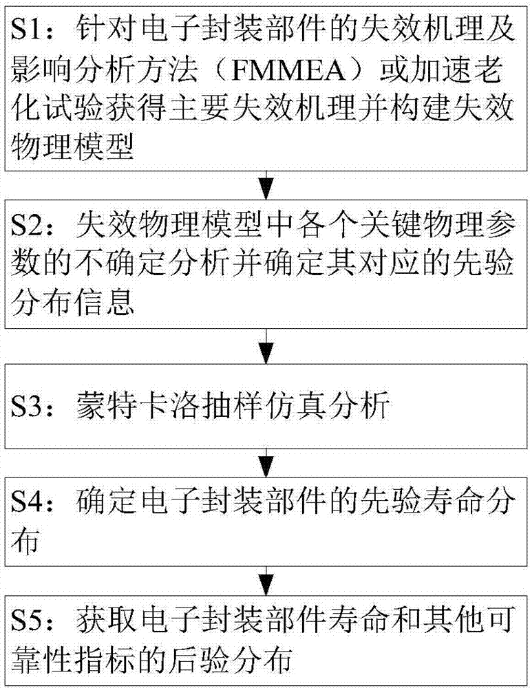
[0022] In order to facilitate those skilled in the art to understand the technical content of the present invention, the present invention will be further explained in conjunction with the accompanying drawings and specific embodiments. It should be understood that the specific embodiments described here are only used to explain the present invention, not to limit the present invention.

[0023] The failure physical model of components can be used to describe the relationship between the failure time of components and various influencing factors that cause component failure. Therefore, establishing a failure physical model of solder joints of multi-chip components can be used to analyze the relationship between various internal and external factors on the fatigue life of solder joints. However, each parameter in the failure physics model is not deterministic, but is affected by various uncertain factors instead. For example, the variability of the material properties itself, ...


PUM


Abstract

The invention discloses a method for analyzing fatigue life of an electronic packaging welding spot. According to the method, with the fatigue life prediction problem of a multi-chip assembly welding spot under a thermal cycle load as a starting point, a probability failure physical modeling frame is analyzed and constructed; a strategy of step-by-step implementation of all key steps is elaborated in details and a strategy of carrying out fusion of life data measured by the test by using the Bayesian theory is explained emphatically, and then a Bayesian information update frame is built. Fitting is carried out based on prior distribution of key parameter uncertainty in an obtained model and the obtained welding spot prior life distribution becomes wide and deviation to a practical measurement value occurs; under the framework of the Bayesian theory, fusion with practically measured data of thermal cycling is carried out and thus centralized welding spot posterior life distribution matching the practical situation well is obtained.

Description

technical field [0001] The invention belongs to the technical field of system reliability analysis and life evaluation, and in particular relates to an analysis method based on a failure physics analysis method and a Bayesian update theory for electronic packaging solder joints affected by internal and external factors on their life. Background technique [0002] The current microelectronic packaging is developing towards lighter, thinner, more cost-effective and more reliable. As the most advanced packaging form today, multi-chip modules are gradually being widely used in military equipment, aerospace components, automotive electronic components, industrial equipment and electronic system products. Multi-Chip Module (MCM) is an emerging high-density three-dimensional packaging technology developed on the basis of hybrid microcircuit thin-thick film technology. It is a high-density mounting and interconnection of multiple integrated circuit bare chips on multiple Layer wiri...

Claims


Application Information

Patent Timeline
IPC IPC(8): G01R31/28G06F17/50
CPCG01R31/2874G06F30/398
Inventor 黄洪钟黄承赓郭来小李彦锋殷毅超郭骏宇米金华
Owner UNIV OF ELECTRONICS SCI & TECH OF CHINA
Why Eureka
Try Eureka