Device and calibration method for overlay error detection
A technology of overlay error and overlay mark, which is applied in the direction of photolithography exposure device, microlithography exposure equipment, photoplate process of pattern surface, etc., can solve the problems of large overlay measurement error and low precision, and achieve Reduction of correlation and improvement of overlay measurement accuracy
- Summary
- Abstract
- Description
- Claims
- Application Information
AI Technical Summary
Problems solved by technology
Method used
Image
Examples
Embodiment 1
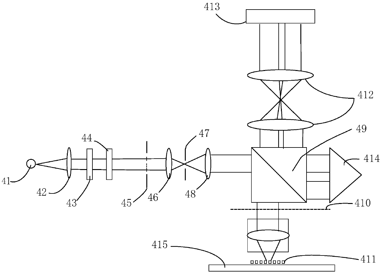
[0067] In this embodiment, the overlay mark 411 itself is used as a reference mark, and the reference mark is obtained by adding overlay signals of the overlay mark 411 at 0 and 180 degrees.
[0068] Specifically, please refer to Figure 9 , the way to obtain the reference signal is:
[0069] When the overlay mark 411 is 0 degrees, the detector 413 receives the measurement light m and the monitoring light s, and performs light intensity disturbance normalization processing on the measurement light m and the monitoring light s to obtain the overlay signal OV_0 at 0 degrees;
[0070] Next, after the rotatable workpiece table 415 drives the overlay mark 411 to rotate 180 degrees, the detector 413 receives the measurement light m and the monitoring light s again, and performs light intensity perturbation normalization processing on the measurement light m and monitoring light s to obtain Overlay signal OV_180 at 180 degrees;
[0071] Then, add the overlay signals of the overlay ...
Embodiment 2
[0080] In this embodiment, a grating mark having the same period as the overlay mark on the test silicon wafer is used as a reference mark. There are two schemes for generating reference marks; one scheme is exactly the same as that in Embodiment 1, and the grating marks on the test silicon wafer are overlaid with signals at 0 degrees and 180 degrees, and added. Another solution is: directly collect the diffraction signal of the grating mark at 0 degrees and perform normalization to obtain the reference signal.
Embodiment 3
[0082] The reference mark in this embodiment uses the grating reference plate installed on the workpiece table. The beam reference plate has grating marks with the same period and direction as the overlay mark, and collects corresponding diffracted light signals according to the difference between the overlay marks. The signal obtained after normalization is the reference signal.
PUM
 Abstract
Description
Claims
Application Information


