

Chip, standby pin switching circuit and switching method thereof
A technology of switching circuits and pins, which is applied in the direction of responding to errors, redundant data in hardware, and error detection, which can solve problems such as scrapping and achieve cost-saving effects
- Summary
- Abstract
- Description
- Claims
- Application Information
AI Technical Summary
Problems solved by technology
Method used
Image

Examples
Embodiment 1
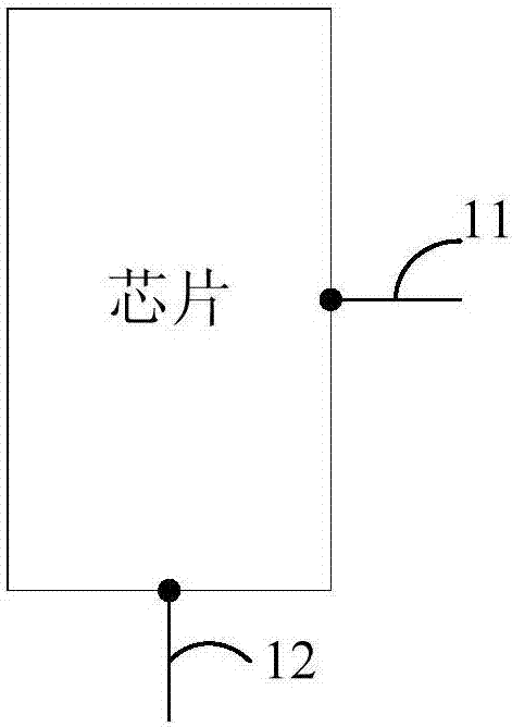
[0026] figure 1 It is a schematic structural diagram of a chip provided by Embodiment 1 of the present invention. Such as figure 1 As shown, the embodiment of the present invention provides a chip, by setting spare pins that meet the functional requirements on the chip, so as to solve the problem that the chip cannot be used normally due to disconnection or damage of the pins during use or debugging.
[0027] The chip includes common pins 11 and spare pins 12 .
[0028] It should be noted that, the spare pins can be selected according to actual needs. Since there is pin multiplexing in general, that is, one pin will be used by multiple devices, even if these devices cannot work at the same time, when selecting a spare pin, it should be considered that the selected spare pin fully meets the actual requirements. Functional Requirements. Exemplary, under normal circumstances, the spare pin we choose should be able to do both GPIO (General Purpose Input Output, general purpose...
Embodiment 2
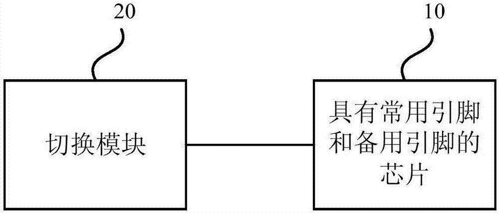
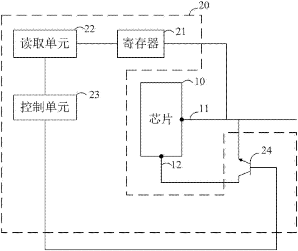
[0032] figure 2 It is a schematic structural diagram of a standby pin switching circuit provided by Embodiment 2 of the present invention, as shown in figure 2 As shown, the spare pin switching circuit includes the chip 10 provided in Embodiment 1 with common pins and spare pins. Preferably, the spare pin switching circuit further includes a switching module 20 .
[0033] The switching module 20 is connected with the chip 10 and is used for switching the pins of the chip 10 from the common pins to the spare pins according to the pin state of the common pins of the chip 10 .
[0034] It should be noted that one end of the switching module is connected to the common pin of the chip, and the other end is connected to the spare pin of the chip. Preferably, one end of the switching module can be connected to multiple common pins of the chip, and the other end can be connected to a spare pin of the chip, when any of the common pins of the chip is broken Or when there is no signa...
Embodiment 3
[0047] see Figure 4 , is a schematic flowchart of a backup pin switching method provided by Embodiment 3 of the present invention. The method is executed by the standby pin switching circuit provided in the embodiment of the present invention, and the steps are as follows:
[0048] S410. When the commonly used pin cannot be registered, it is determined that the pin is in an abnormal state.
[0049] What needs to be said is that when the system restarts and enters the initialization state, the common pins on the chip will be re-registered, and once the system judges that a common pin cannot be registered, the system will start to switch the spare pin Perform the registration operation.
[0050] S420. The control unit forms a control signal according to the abnormal state of the pin, and controls the triode to switch the standby pin according to the control signal, wherein the abnormal state of the pin is stored in a register and read by the reading unit.
[0051] It should be...
PUM
 Abstract
Description
Claims
Application Information