
Flexible display panel, display device and flexible display panel manufacturing method

A technology of flexible display and manufacturing method, which is applied in the directions of identification device, final product manufacturing, climate sustainability, etc., and can solve problems such as display failure and inorganic insulating layer cracks

Active Publication Date: 2017-07-21
BOE TECH GRP CO LTD +1
View PDF5 Cites 48 Cited by
  • Summary
  • Abstract
  • Description
  • Claims
  • Application Information

AI Technical Summary

Problems solved by technology

[0006] Embodiments of the present invention provide a flexible display panel, a display device, and a method for manufacturing a flexible display panel, so as to solve the problem in the prior art of how to avoid cracks in the inorganic insulating layer in the bending area under the condition of relatively low production costs. The problem caused by the display failure phenomenon

Method used


Image

  • Flexible display panel, display device and flexible display panel manufacturing method
  • Flexible display panel, display device and flexible display panel manufacturing method
  • Flexible display panel, display device and flexible display panel manufacturing method

Examples


Embodiment 1

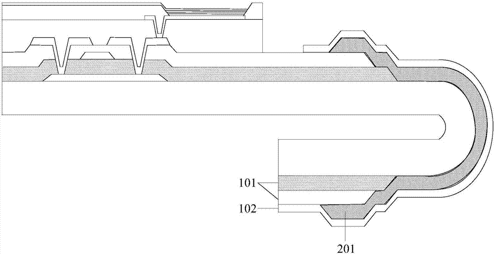
[0048] A flexible display panel provided by Embodiment 1 of the present invention, such as image 3 As shown, it includes: a flexible substrate substrate 301, a conductive layer 302 disposed on the display area A of the flexible substrate substrate, a plurality of wires 303 disposed on the edge bending region B of the flexible substrate substrate, and a plurality of wires 303 disposed on the conductive layer 302 and The inorganic insulating layer 304 between the multiple wiring lines 303 and the flexible substrate 301; the conductive layer 302 is electrically connected to the multiple wiring lines 303 and arranged on the same layer; in particular, the flexible display panel also includes:

[0049] At least the first organic insulating layer 305 is disposed on the edge bending area B of the flexible substrate; the first organic insulating layer 305 is located between the plurality of wires 303 and the inorganic insulating layer 304, and the material of the first organic insulati...

Embodiment 2

[0055] Since the structure of the flexible display panel provided by Embodiment 2 of the present invention is similar to that of the flexible display panel provided by Embodiment 1 of the present invention, only the flexible display panel provided by Embodiment 2 of the present invention and the flexible display panel provided by Embodiment 1 of the present invention are discussed here. The differences will be introduced, and the repetitions will not be repeated.

[0056] According to the above description, in the flexible display panel provided in Embodiment 1 of the present invention, the inorganic insulating layer 304 has a via hole pattern. In practical applications, the conductive layer 302 located at the via hole pattern may be broken, which affects the display effect of the flexible display panel.

[0057] Specifically, in order to prevent the conductive layer 302 from breaking at the via hole pattern, in the above flexible display panel provided in Embodiment 2 of the ...

Embodiment 3

[0060] Since the structure of the flexible display panel provided by the third embodiment of the present invention is similar to that of the flexible display panel provided by the second embodiment of the present invention, only the flexible display panel provided by the third embodiment of the present invention is compared with the flexible display panel provided by the second embodiment of the present invention. The differences will be introduced, and the repetitions will not be repeated.

[0061] Specifically, on the basis of the flexible display panel provided in the second embodiment of the present invention, in order to prevent the multiple traces 303 in the bending area B at the edge of the flexible substrate from being scratched, the above flexible display panel provided in the third embodiment of the present invention display panel, such as Figure 5 As shown, the second organic insulating layer 310 disposed at least at the edge bending area B of the flexible substrat...


PUM


Abstract

The invention discloses a flexible display panel, a display device and a flexible display panel manufacturing method. The flexible display panel comprises a flexible substrate, a conductive layer in a display area of the flexible substrate, multiple lines in an edge bending area of the flexible substrate, and an organic insulating layer between the conductive layer and the multiple lines on one hand and the flexible substrate on the other hand. The flexible display panel further comprises a first organic insulating layer at least arranged between the multiple lines in the edge bending area of the flexible substrate and the organic insulating layer. The first organic insulating layer is made of cured photoresist. As the first organic insulating layer made of cured photoresist can prevent cracks produced by the inorganic insulating layer from spreading to the multiple lines, the phenomenon of display failure is avoided. In specific implementation, the photoresist can be photoresist applied in the making process of the inorganic insulating layer. Therefore, two Mask processes are omitted, the production cost is saved, and the production efficiency is improved.

Description

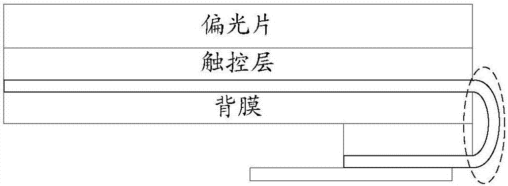
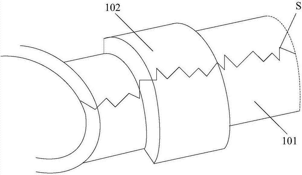
technical field [0001] The present invention relates to the field of display technology, in particular to a flexible display panel, a display device and a method for manufacturing the flexible display panel. Background technique [0002] The display market is currently booming, and more new displays will emerge in the future as consumer demand continues to increase for a wide variety of display products such as laptops, smartphones, TVs, tablets, smart watches, and fitness wristbands product. [0003] Full-screen borderless display products can enable users to obtain a better viewing experience, and will surely detonate a new consumer market. Pad Bending is the core technology of full-screen borderless display products. However, if Figure 1a with Figure 1b As shown, due to the high brittleness of the inorganic insulating layer 101 , Pad Bending will cause a crack S to occur in the inorganic insulating layer 101 in the bending area of ​​the display product, and the crack...

Claims


Application Information

Patent Timeline
Patent Type & Authority Applications(China)
IPC IPC(8): H01L27/12H01L27/32H01L21/77
CPCH01L27/1244H01L27/1248H01L27/1259H10K59/124H10K59/131Y02E10/549Y02P70/50H10K77/111G09F9/301
Inventor 黄炜赟刘庭良
Owner BOE TECH GRP CO LTD
Learn More