Chip scale package light-emitting apparatus having recessed design and manufacturing method thereof

A light-emitting device and manufacturing method technology, applied in the direction of electrical components, circuits, semiconductor devices, etc., can solve the problems of reduced reliability, electrical connection failure, high energy consumption of LEDs, etc., to improve welding failure or poor welding quality, and avoid electrical connection The effect of failure

Active Publication Date: 2017-07-25
MAVEN OPTRONICS CO LTD
View PDF3 Cites 9 Cited by
  • Summary
  • Abstract
  • Description
  • Claims
  • Application Information

AI Technical Summary

Problems solved by technology

However, in the process of reflow soldering or eutectic bonding of existing CSP LEDs, the packaging structure covering the LED chip will expand due to heat; the expanded packaging structure will contact and push the substrate below it, which will cause LED damage. There is a large gap between the electrode and the pad of the substrate
This situation will cause the LED to not be properly soldered to the substrate, resulting in electrical connection failure or poor soldering quality, and the latter will cause higher electrical and thermal resistance,

Method used


Image

  • Chip scale package light-emitting apparatus having recessed design and manufacturing method thereof
  • Chip scale package light-emitting apparatus having recessed design and manufacturing method thereof
  • Chip scale package light-emitting apparatus having recessed design and manufacturing method thereof

Examples


Embodiment Construction

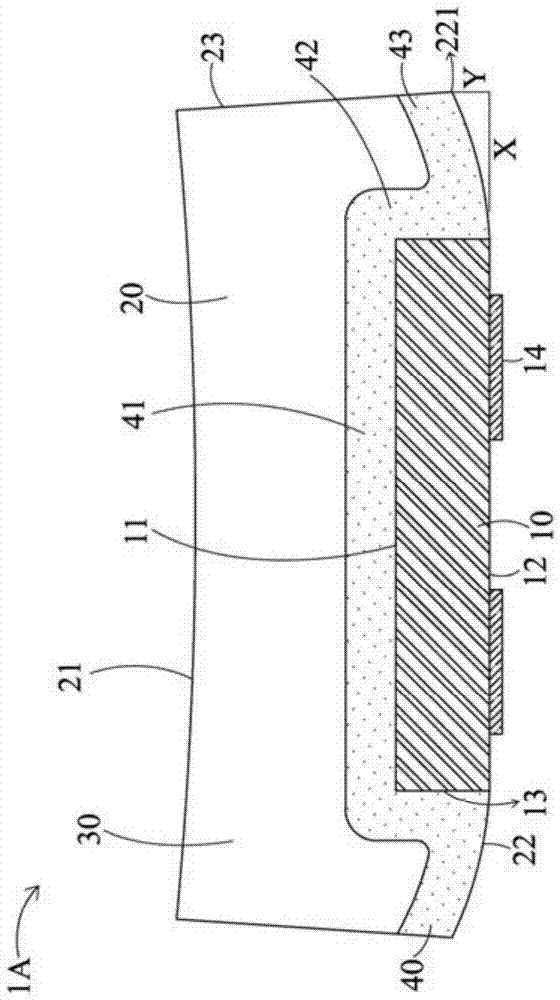
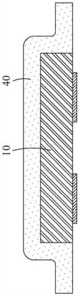
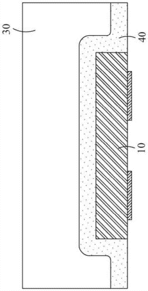
[0067] see Figure 1A As shown, it is a schematic diagram (sectional view) of a light emitting device (light emitting device, LED) according to the first preferred embodiment of the present invention. The light emitting device 1A may include an LED chip 10 and a wrapping structure 20 , and the technical content of these elements will be described in sequence as follows.

[0068] The LED chip 10 is a flip-chip LED chip, and can have an upper surface 11 , a lower surface 12 , a vertical surface 13 and an electrode group 14 in appearance. The upper surface 11 and the lower surface 12 are oppositely disposed, and the vertical surface 13 is formed between the upper surface 11 and the lower surface 12 and connects the upper surface 11 and the lower surface 12 . The electrode group 14 is disposed on the lower surface 12 and may have more than two electrodes. Electric energy (not shown in the figure) can be supplied into the LED chip 10 through the electrode group 14, and then the L...


PUM


Abstract

The invention provides a chip scale package light-emitting apparatus having recessed design and a manufacturing method thereof. The chip scale package light-emitting apparatus includes a flip chip type LED chip and a cladding structure. The cladding structure covers the LED chip, and has a bottom surface warps upwardly to for a recessed shape. The invention also provides a manufacturing method for manufacturing the light-emitting apparatus. The apparatus and the method can avoid or improve poor quality of welding points between the light-emitting apparatus and a substrate which is often caused by greater gap between an electrode group of the LED chip and a welding pad of the substrate due to expansion of the cladding structure upon being heated in reflow soldering or eutectic bonding. Therefore, the apparatus and the method can secure the electrode group to the substrate. With excellent welding quality, failure of electrical connection of the light-emitting apparatus can be avoided, the thermal resistance between the light-emitting apparatus and the substrate can be lowered, temperature at the binding point can be lowered when the light-emitting apparatus operates, and light-emitting efficiency and reliability can be improved.

Description

technical field [0001] The present invention relates to a light emitting device (light emitting device, LED) and a manufacturing method thereof, in particular to a chip scale packaging (CSP) light emitting device with a concave design and a manufacturing method thereof. Background technique [0002] LED (light emitting device) is commonly used to provide lighting sources or configured in electronic products as display light sources or indicator lights, and LED chips are usually placed in a bracket-type or ceramic substrate-type package structure, and are covered by a fluorescent The material wraps or covers to become a light emitting device (LED). The light-emitting device can be fixed to other structures such as a substrate by reflow soldering or eutectic bonding, so that electric energy can be transmitted through the substrate to drive the light-emitting device to emit light. [0003] With the evolution of LED technology, chip scale packaging (CSP) light-emitting devices ...

Claims


Application Information

Patent Timeline
IPC IPC(8): H01L33/48H01L33/52H01L33/54H01L33/56H01L33/00
CPCH01L33/48H01L33/52H01L33/54H01L33/56H01L2933/005
Inventor 陈杰王琮玺钟君炜
Owner MAVEN OPTRONICS CO LTD
Why Eureka
Try Eureka