
Method for protecting fine pattern and depositing metal layer using back exposure technology

A technology of backside exposure and metal layer, applied in microlithography exposure equipment, photolithography process exposure devices, etc., can solve the problems of consistent patterns and difficult patterns, and achieve the effect of saving manufacturing time and cost, and reducing film stress.

Active Publication Date: 2019-09-27
KOREA INST OF IND TECH
View PDF2 Cites 0 Cited by
  • Summary
  • Abstract
  • Description
  • Claims
  • Application Information

AI Technical Summary

Problems solved by technology

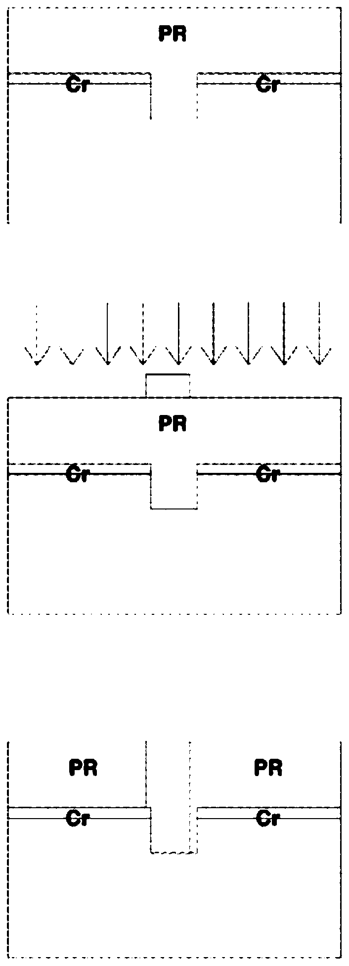
[0007] However, if figure 1 In the example in , the pattern formation of the post-process is to use the exposure in the upper direction, so it is difficult for the pattern formed by the post-process to be consistent with the original pattern

Method used


Image

  • Method for protecting fine pattern and depositing metal layer using back exposure technology
  • Method for protecting fine pattern and depositing metal layer using back exposure technology
  • Method for protecting fine pattern and depositing metal layer using back exposure technology

Examples


Embodiment Construction

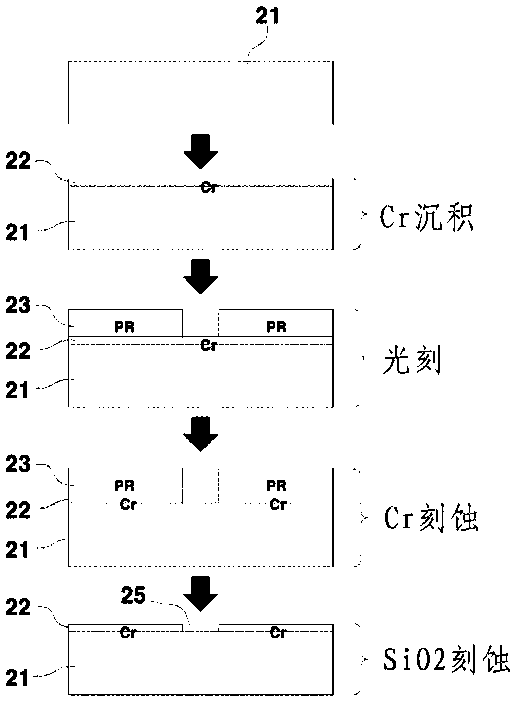
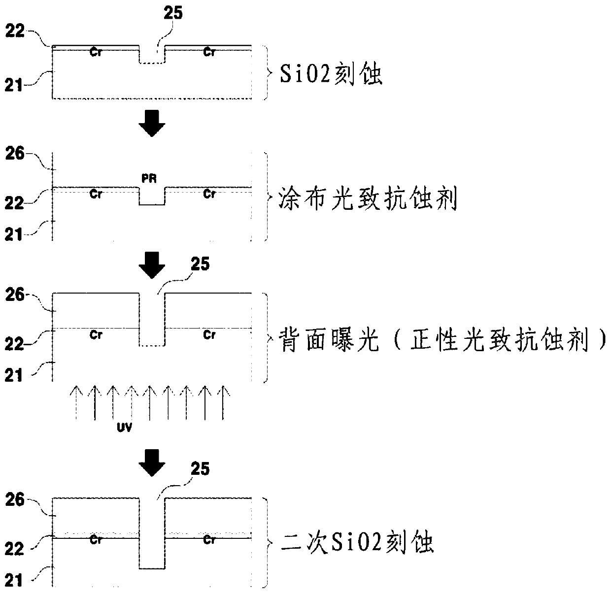
[0077] Through the above-mentioned backside exposure process of the optical element and the like of the present invention, the fine pattern of the optical element can be protected, and at the same time, the metal mask layer can be easily deposited. The following are related examples.

[0078] That is, the transparent substrate 21 is preferentially prepared. Such a transparent substrate 21 forms a photoresist, a metal layer, etc. substantially on the upper surface, and constitutes a base of components.

[0079]And, as shown in the figures and the following description, elements such as optical elements, semiconductor layers, and display panels are manufactured through a plurality of processes. Therefore, the present invention implements back exposure in this process, so that additional processing of the pattern holes formed on the transparent substrate can be realized, and the metal layer can be easily formed again on the upper part of the metal layer, while having the advantag...


PUM

PropertyMeasurementUnit
thicknessaaaaaaaaaa

Abstract

The present invention relates to a method for protecting a micropattern and depositing a metal layer using backside illumination technology, which allows a photoresist metal layer to be deposited on a transparent substrate and a metal layer in a state where a predetermined pattern is formed thereon while protecting a pattern that has already been formed, without alignment error and without using an optical device mask for an additional process, and which also allows post processing to be performed so as to match an existing pattern hole when performing additional etching for the pattern that has already been processed on the transparent substrate, thereby enabling precise post processing. The present invention as described above is characterized by comprising: an etching step of etching a metal layer and a transparent substrate using a photoresist comprising a predetermined pattern with respect to the metal layer formed on the transparent substrate to thereby form a pattern hole on the metal layer and the transparent substrate, or forming a pattern hole on the metal layer by etching the metal layer; a backside illumination preparation step of applying a photosensitive material onto the metal layer and the pattern hole with the predetermined pattern being formed therein by etching; and a backside illumination step of eliminating a part of the photosensitive material by backside illumination at the transparent substrate side, wherein the photosensitive material is formed of a positive photoresist, and the photosensitive material is eliminated from the predetermined pattern hole through the backside illumination step. The backside illumination step is followed by an additional etching step of etching the transparent substrate in the predetermined pattern hole from which the photosensitive material has been eliminated.

Description

technical field [0001] The present invention relates to a method of protecting a fine pattern and depositing a metal layer using back exposure technology, which does not use an optical element mask for an additional process in a state where a predetermined pattern is formed on a transparent substrate and a metal layer, and there is no alignment Deposition of photoresist and metal layer while protecting the already formed pattern from errors, and when additional etching is performed on the pattern processed on the transparent substrate, post-processing can be performed in conformity with the existing pattern hole, thereby enabling Realize precise post-processing. Background technique [0002] Generally, transparent substrates are commonly used for optical elements, display panels, and the like. By laminating and coating metal layers or resin layers on such a transparent substrate, a predetermined pattern is formed to utilize the characteristics of the device. [0003] A plu...

Claims


Application Information

Patent Timeline
Patent Type & Authority Patents(China)
IPC IPC(8): G03F7/20
Inventor 金泳百河泰元郑砚宅许起锡
Owner KOREA INST OF IND TECH
Learn More