

Method for removing dielectric layer on surface of metal layer at top of semiconductor device
A surface dielectric layer and optical device technology, which is applied in semiconductor devices, semiconductor/solid-state device manufacturing, electrical components, etc., can solve problems such as inability to scratch, short circuit between reflective metal patterns, and affect device display performance, so as to avoid metal surface Scratches, the effect of reducing production costs
- Summary
- Abstract
- Description
- Claims
- Application Information
AI Technical Summary
Problems solved by technology
Method used
Image

Examples
Embodiment Construction
[0026] In order to make the above objects, features and advantages of the present invention more comprehensible, specific implementations of the present invention will be described in detail below in conjunction with the accompanying drawings.
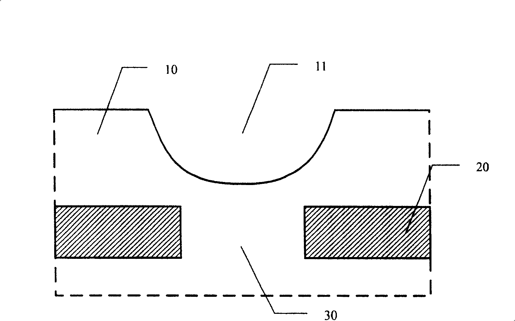
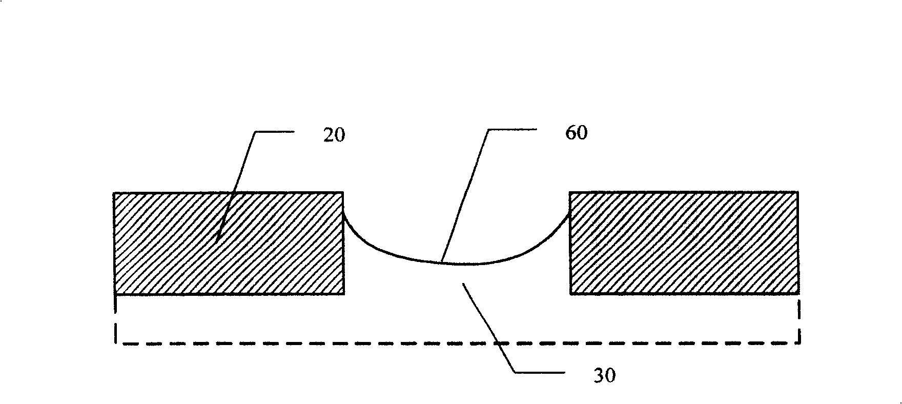
[0027] The reverse etching technology forms a sacrificial layer on the surface of the dielectric material with surface undulations to fill the lower part of the surface, and then uses etching technology to etch the sacrificial layer and the dielectric material. By controlling the etching rate of each part of the material to be flattened, the surface Planarize and make the etched sacrificial layer and dielectric material reach the required thickness.
[0028] The process of applying the method of the present invention to remove the dielectric layer on the surface of the metal layer on the top of the semiconductor optical device is as follows: first, according to the process requirements, a dielectric layer is formed on the surface of the...
PUM
 Abstract
Description
Claims
Application Information