

Touch display panel and touch display device
A touch display panel, touch technology, which is applied to instruments, computing, electrical and digital data processing, etc., can solve the problems of poor bending of OLED display panels, multiple layers of OLED display panels, and large thickness of display panels, etc. Transmittance, increase in anti-reflection performance, and achieve the effect of thinning
Active Publication Date: 2017-08-11
SHANGHAI TIANMA MICRO ELECTRONICS CO LTD +1
View PDF5 Cites 9 Cited by
- Summary
- Abstract
- Description
- Claims
- Application Information
AI Technical Summary
Problems solved by technology
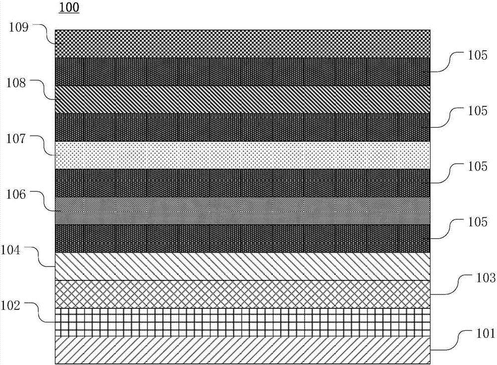
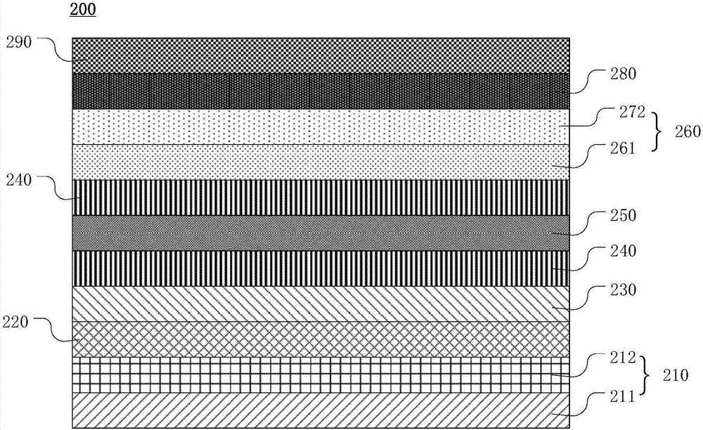
[0006] It can be seen that in the prior art, the OLED display panel with an external mutual capacitive touch film has more stacked structures, resulting in a larger thickness of the entire display panel.
When applied to flexible OLED products, due to the larg
Method used
View moreImage
Smart ImageViewing Examples

Examples
 PUM
 Abstract
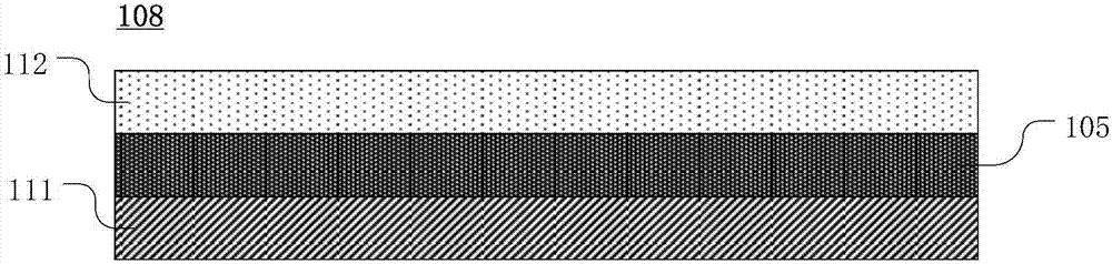
The invention provides a touch display panel and a touch display device. The touch display panel comprises a first substrate, a display element, a compound film and an optimal film, wherein the display element is positioned on the first substrate; the compound film is positioned on the display element and comprises at least one barrier layer and a first touch electrode layer, wherein the first touch electrode layer comprises a plurality of first touch electrodes; and the optical film is positioned on the compound film and comprises a 1/2 phase-difference film and a second touch electrode layer, wherein the second touch electrode layer is arranged on the 1/2 phase-difference film, the second touch electrode layer and the first touch electrode layer are insulated, and the second touch electrode layer comprises a plurality of second touch electrodes. By use of the touch display panel and the touch display device provided by the invention, the thinning of the touch display panel can be realized.
Description
technical field [0001] The present invention relates to the field of display technology, in particular to a touch display panel and a touch display device. Background technique [0002] With the development of human-computer interaction technology, touch technology is increasingly used on various displays. Capacitive touch technology is widely used due to its advantages of wear resistance, long life, low maintenance cost for users, and support for gesture recognition and multi-touch. [0003] Capacitive touch technology can be divided into self-capacitive touch technology and mutual-capacitive touch technology according to the detection method of capacitance between different objects. Self-capacitive touch technology detects the presence, position, and motion of an input object on a touch screen based on changes in capacitance between the input object and electrodes. The mutual capacitive touch technology detects the existence, position and movement of an input object on t...
Claims
Login to View More Application Information
Patent Timeline
 OwnerSHANGHAI TIANMA MICRO ELECTRONICS CO LTD