Single-photon avalanche photodiode time-delay integration cmos image sensor
A time delay integration, photodiode technology, applied in image communication, television, electrical components, etc., can solve problems such as insufficient detection ability, and achieve the effect of global exposure, low pressure, and consistency.
- Summary
- Abstract
- Description
- Claims
- Application Information
AI Technical Summary
Problems solved by technology
Method used
Image

Examples
Embodiment Construction
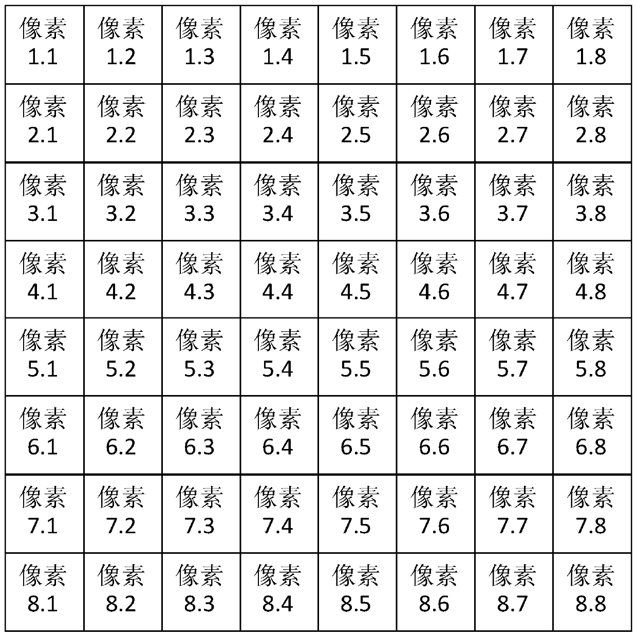
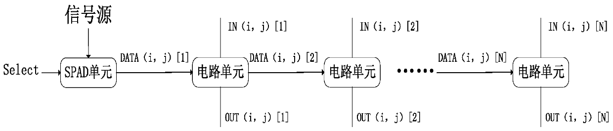
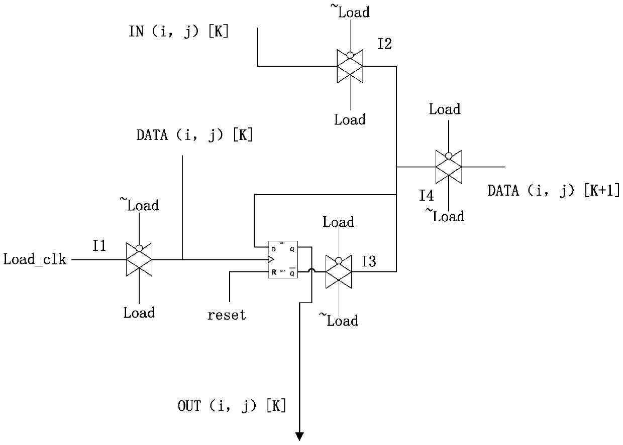
[0013] The system circuit structure diagram is as follows figure 1 As shown, the matrix of X multiplied by Y is formed by the arrangement of square pixels, and the internal circuit structure diagram of the i-th row and j-th column pixel is as follows figure 2 As shown, it is composed of SPAD unit and circuit unit. Taking N-bit output precision as an example, the SPAD unit is controlled by the select signal to convert the external signal source into a pulse signal. A pixel has N circuit units in total. Taking the Kth unit as an example, it is connected to IN(i, j)[k], OUT(i, j)[k], DATA(i, j)[k], DATA(i,j)[k+1] four signals, where OUT(i,j)[k]=IN(i+1,j)[k]. Its internal structure diagram is as follows Figure 4 shown. It is composed of D flip-flop and transmission gate with reset function. IN(i,j)[k] is connected to the input terminal of transmission gate I2, the output terminal of I2 is connected to the D terminal of the D flip-flop, DATA(i,j)[k] is connected to the clock ...
PUM
 Abstract
Description
Claims
Application Information