Defect inspection method and defect inspection device for wide bandgap semiconductor substrate

A defect inspection, wide bandgap technology, applied in semiconductor/solid-state device testing/measurement, optical test defect/defect, material excitation analysis, etc.

Active Publication Date: 2020-12-29
TORAY ENG CO LTD
View PDF8 Cites 0 Cited by
  • Summary
  • Abstract
  • Description
  • Claims
  • Application Information

AI Technical Summary

Problems solved by technology

However, SiC epitaxial substrates still have a large number of defect crystals, so they need to be fully inspected in order to use them as power semiconductor devices

Method used


Image

  • Defect inspection method and defect inspection device for wide bandgap semiconductor substrate
  • Defect inspection method and defect inspection device for wide bandgap semiconductor substrate
  • Defect inspection method and defect inspection device for wide bandgap semiconductor substrate

Examples


Embodiment Construction

[0103]

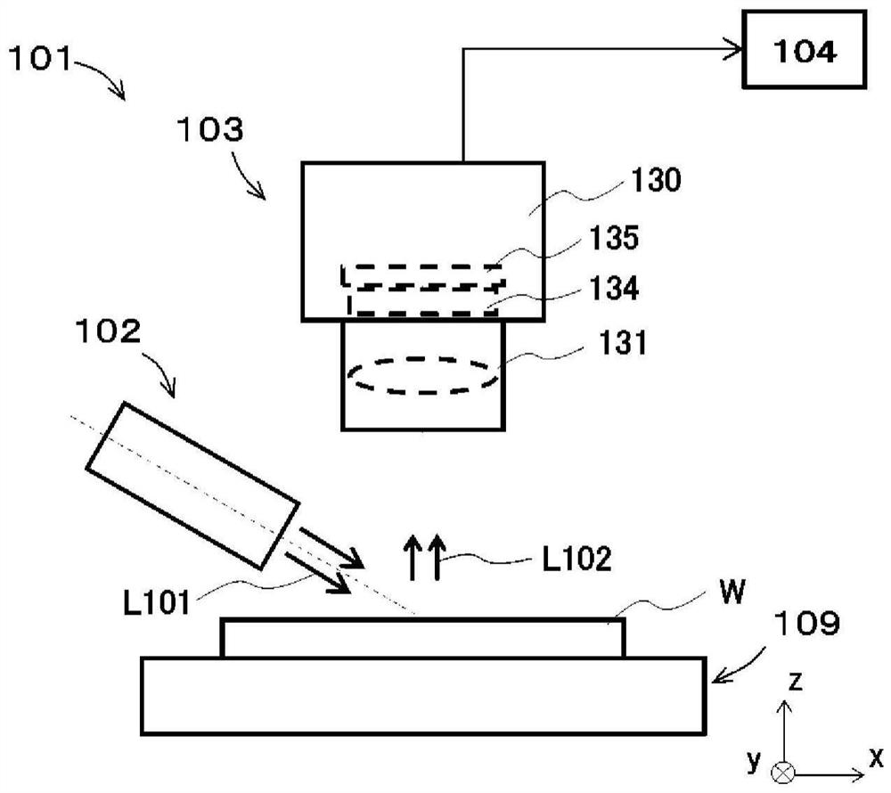
[0104] Hereinafter, a first embodiment for carrying out the present invention will be described.

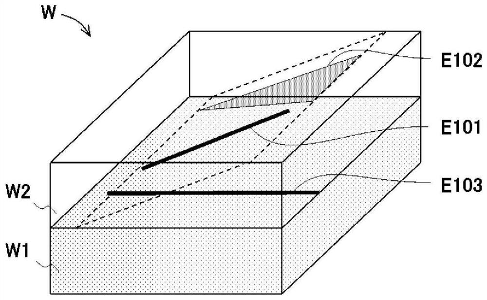
[0105] The defect inspection method of the present invention is a method for inspecting defects generated in a wide bandgap semiconductor substrate,

[0106] Excitation light is irradiated toward the wide bandgap semiconductor substrate,

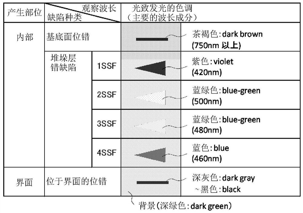
[0107] Photographs photoluminescence in the visible light region emitted when excitation light is irradiated onto a wide-bandgap semiconductor substrate,

[0108] Based on the intensity of light emitted from a portion of a wide-bandgap semiconductor substrate including a defect to be inspected in a captured image including photoluminescence in the visible light region and the intensity of light emitted from a portion of the wide-bandgap semiconductor substrate that does not include a defect as The difference in the intensity of light emitted from the portion of the defect to be inspected is used to inspect the defect generated in the ...


PUM


Abstract

The purpose of the present invention is to provide a method and a defect inspection device for quickly and reliably inspecting wide-gap semiconductor substrates for defects, despite a device configuration that is simple. Specifically, there are provided a method or a defect inspection device for inspecting a wide-gap semiconductor substrate for defects, characterized in that excitation light is irradiated towards the wide-gap semiconductor substrate; photoluminescence in the visible light region emitted due to irradiation of the wide-gap semiconductor substrate by the excitation light is photographed; and an inspection of defects occurring in the wide-gap semiconductor substrate is carried out on the basis of the difference between the intensity of light emitted from defect-free regions of the wide-gap semiconductor substrate and the intensity of light emitted from defect regions of the wide-gap semiconductor substrate, in the photographed image which includes the photoluminescence in the visible light region.

Description

technical field [0001] The present invention relates to a method and an apparatus for inspecting defects generated in an epitaxial layer formed on a wide bandgap semiconductor substrate or in the material itself constituting the wide bandgap semiconductor substrate. Background technique [0002] A structure in which an epitaxial layer is formed on a SiC substrate (so-called SiC epitaxial substrate) is a wide-bandgap semiconductor, and it is a power semiconductor device that is attracting attention with the spread of solar power generation, hybrid vehicles, and electric vehicles. However, SiC epitaxial substrates still have a large number of defect crystals, so they need to be fully inspected in order to use them as power semiconductor devices. [0003] Among them, crystal defects called basal plane dislocations (dislocations) are responsible for the propagation of stacking fault defects, which are the cause of deterioration of the forward characteristics of pn junction diode...

Claims


Application Information

Patent Timeline
Patent Type & Authority Patents(China)
IPC IPC(8): G01N21/64G01N21/88H01L21/66
CPCG01N21/64G01N21/88
Inventor 村田浩之大槻真左文
Owner TORAY ENG CO LTD
Why Eureka
Try Eureka