Integrated circuits design

a technology of integrated circuits and integrated circuits, applied in the field of integrated circuit design, can solve the problems of increasing the complexity of the integrated circuit, the complexity of the i/o ring has to compensate, and the number of i/o pins on the package has not been keeping pa

Active Publication Date: 2011-05-19
ARM IRELAND LTD
View PDF3 Cites 15 Cited by
  • Summary
  • Abstract
  • Description
  • Claims
  • Application Information

AI Technical Summary

Benefits of technology

[0102]the order of prioritization of signals into the second stage multiplexer is based on priority of control.

Problems solved by technology

While integrated circuit functional complexity keeps growing, the number of I / O pins on a package hasn't been keeping pace, and the complexity of the I / O ring has had to compensate.
Increasing gate density allows more functionality to be implemented in these devices and the number of available pins imposes limitations.
With increasing I / O layer complexity, device pins are heavily bound within a pin-limited package.
The internal chip core functions may require two to four times the number of available device pins leading, to complex many-to-many multiplexing scenarios.
Some approaches exist in the industry which use time-division multiplexing to reduce the number of pins between devices, but where chips need to connect to specific devices, this approach is not satisfactory.
I / O cells themselves are becoming more complex and therefore require more fine grained control to account for process, voltage and temperature variation in the manufacturing process and operating conditions of the device.
In a power-sensitive device the physical view of the system is very different to the functional view and this can seriously impact the chip infrastructure as low power design techniques require rethinking of the entire IC design flow.
When considering that the granular multiplex and control circuitry for a single chip pin may be extensive, the problem is exacerbated when there are hundreds or thousands of pins and where the requirements may change frequently.
Manual coding of incrementally changing I / O requirements leads to poorer design quality and high consumption of design resources to design and verify the I / O ring.
Also the turn-around time between a requirements (specification) change and a resulting change in the I / O ring implementation (circuitry) could be excessive.
This falls down however when a chip has to be connected to different devices that may not be aware of any pin sharing protocols.

Method used


Image

  • Integrated circuits design
  • Integrated circuits design
  • Integrated circuits design

Examples


Embodiment Construction

Brief Description of the Drawings

[0103]The invention will be more clearly understood from the following description of some embodiments thereof, given by way of example only with reference to the accompanying drawings in which:—

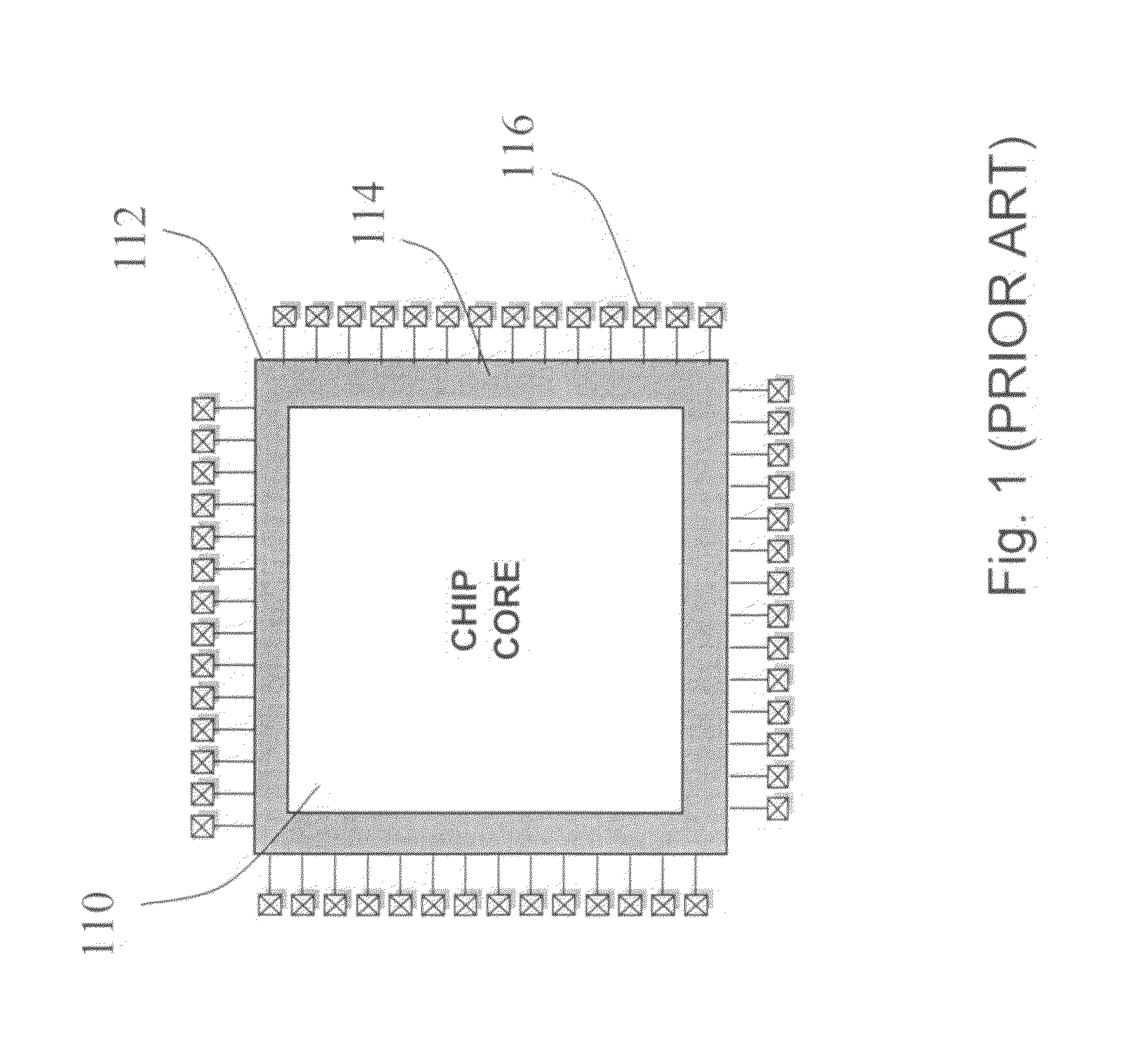
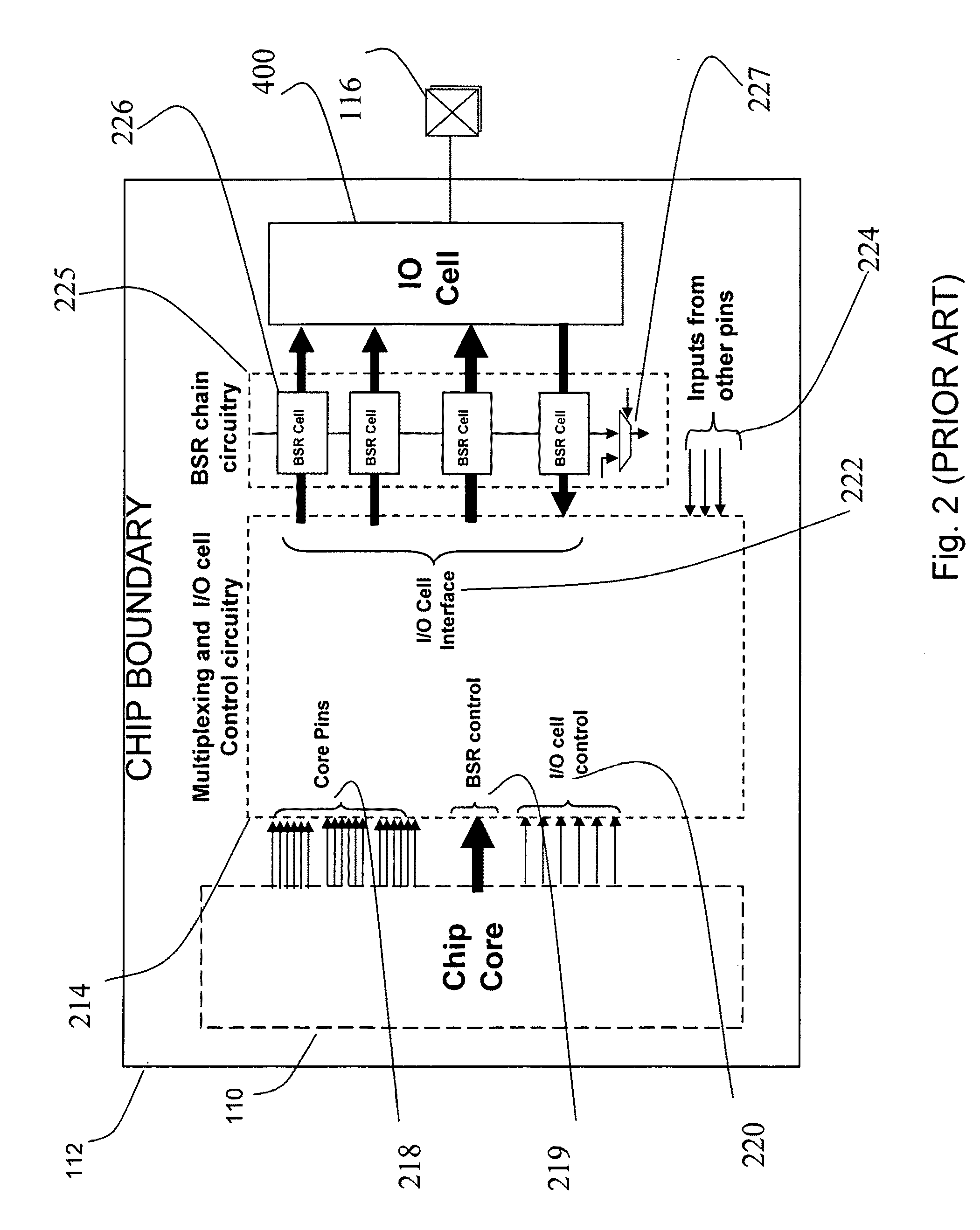
[0104]FIGS. 1, 2, 3 and 4 are diagrams representing the prior art, as discussed above;

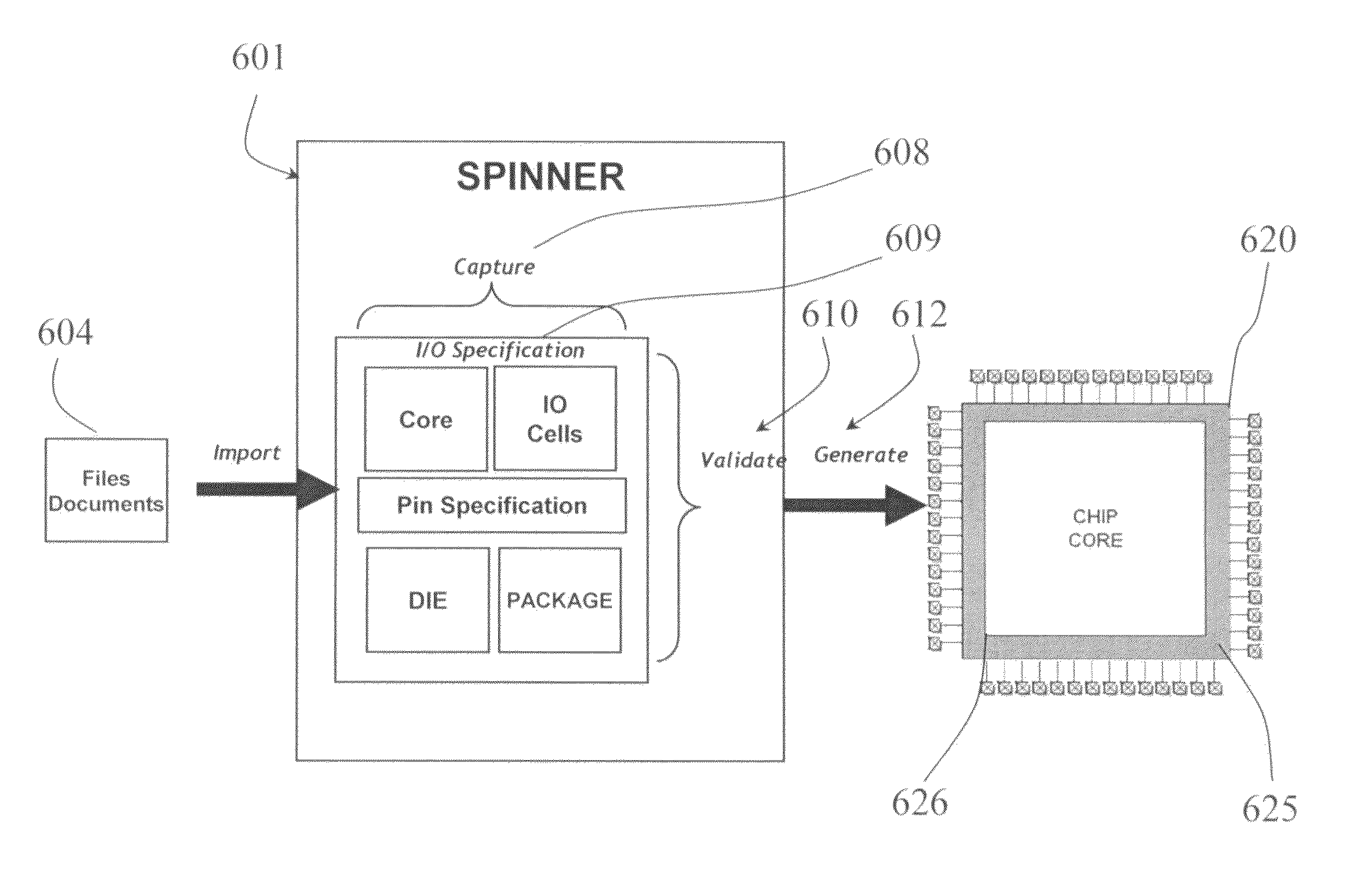
[0105]FIG. 5 is a flow diagram illustrating at a high level operation of a tool for importing IC requirement documents, allowing the user to capture additional I / O specification information and to generate an I / O fabric design with a high level of automation;

[0106]FIGS. 6, 7 and 8 are high level view of a generic pin muxing structure part of an I / O ring developed by the tool, including both input and output multiplexing (“muxing”);

[0107]FIG. 9 is a circuit diagram showing the preferred embodiment of the mux arrangements for delivering output and output enable logic to an I / O cell;

[0108]FIG. 10 is circuit diagram showing the type of IO Control Override logic which can be plac...


PUM


Abstract

This invention concerns an automated method of generating a design for an I/O fabric of a target integrated circuit having a core and pins. A process tool executes algorithms to generate a synthesizable representation of the I/O fabric ring in hardware description language. It imports integrated circuit design data, and from it captures I/O specification data for a circuit core, library of cells, pin, I/O control, BSR and I/O cell chaining, and die. The tool validates the specification data, and generates the I/O fabric design by configuring and inter-connecting a pin multiplexing and control matrix structures according to constraints for signal control, and timing. The structures includes on both the input and output paths of each pin a functional multiplexer matrix structure, a test multiplexer matrix structure, an override matrix structure, a multiplex select and control matrix structure, and an I/O Cell control logic. A required pin output circuit is configurable by modification of the I/O specification data, and/or, modification of a manner of wiring the algorithms, and/or by modification of the algorithms. The tool wires algorithms according to a wiring framework, and said wiring framework is modifiable.

Description

FIELD OF THE INVENTION[0001]The invention relates to design of integrated circuits and to end-product integrated circuits.PRIOR ART DISCUSSION[0002]FIG. 1 shows a typical integrated circuit 112 at a high level. The chip 112 contains an internal logic core 110, an I / O ring 114, and pins 116. FIG. 2 shows the logic interfaces between the core 110 and a single chip pin 116. The chip pin 116 is connected physically to an I / O cell 400 (FIG. 3), which fulfills a wide range of requirements for connecting to the environment external to the chip in a correct manner. This I / O cell 400 has a chip side interface 222 that can be used to control the I / O cell and may range from a simple output signal to a full suite of control capability including characteristics such as timing, slew-rate, output drive, pull-up / pull-down, and power. On the chip core 110 side the interfaces to I / O logic can include core signals that can be selected as device pins 218, control for Boundary Scan circuitry and registe...

Claims


Application Information

Patent Timeline
Patent Type & Authority Applications(United States)
IPC IPC(8): G06F17/50
CPCG06F17/505G06F30/327
Inventor MURRAY, DAVIDBOYLAN, SEAN
Owner ARM IRELAND LTD
Why Eureka
Try Eureka