Unlock instant, AI-driven research and patent intelligence for your innovation.
Electronic sandwich structure with two parts joined together by means of a sintering layer with alternating regions of higher and lower density and corresponding manufacturing method
What is Al technical title?
Al technical title is built by PatSnap Al team. It summarizes the technical point description of the patent document.
A sandwich structure, sintered layer technology, applied in semiconductor/solid-state device manufacturing, circuits, electrical components, etc., can solve the problems of mismatch, insufficient elasticity of the silver sintered layer, damage to the integrity of the silver sintered layer, etc., to achieve high reliability and reliability. soft effect
Active Publication Date: 2017-08-29
DANFOSS SILICON POWER
View PDF4 Cites 0 Cited by
Summary
Abstract
Description
Claims
Application Information
AI Technical Summary
This helps you quickly interpret patents by identifying the three key elements:
Problems solved by technology
Method used
Benefits of technology
Problems solved by technology
In these cases, the elasticity of the silver sintered layer is insufficient and the mismatch results in shear stresses, which may end in destroying the integrity of the silver sintered layer or the contact layer of one part to be bonded
Method used
Image
Click on the blue label to locate the original text in one second.
Reading with bidirectional positioning of images and text.
Examples
Embodiment Construction
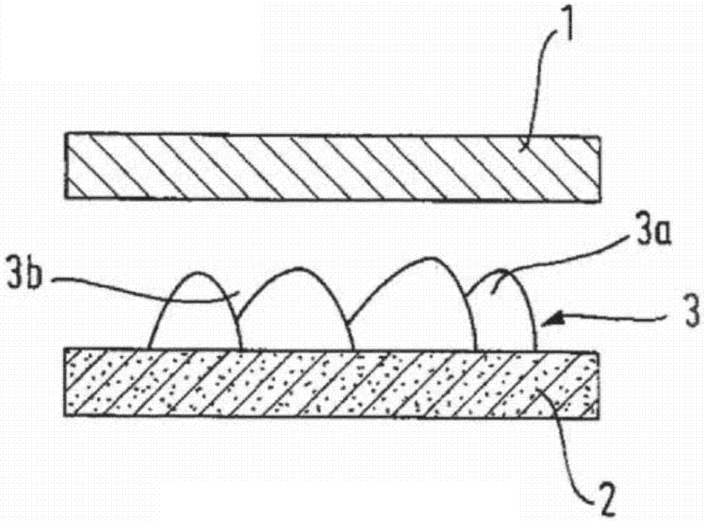
[0034] in Figure 1a In ), the sintered material layer 3 arranged between the first part to be joined 1 and the second part to be joined 2 presents a basic arrangement. The sintered material layer is in the form of a relatively slightly free-flowing or pasty sintered paste applied to the second part to be bonded on the surface of the second part to be bonded 2 or facing the bonding surface of the first part to be bonded . In this case, the sintered paste has been applied in the form of dots, thereby presenting a region 3a with a larger thickness and a region 3b with a smaller thickness before sintering. When applied, the sintered paste has a viscous consistency that is sufficiently high in viscosity that the single "pile" applied in dots and forming the first height profile does not fully polymerize. In this state, the drying of the sintered paste also occurs before sintering, so that Figure 1a The form of the sintered material layer indicated in) basically corresponds to the f...
PUM
Property
Measurement
Unit
thickness
aaaaa
aaaaa
thickness
aaaaa
aaaaa
Abstract
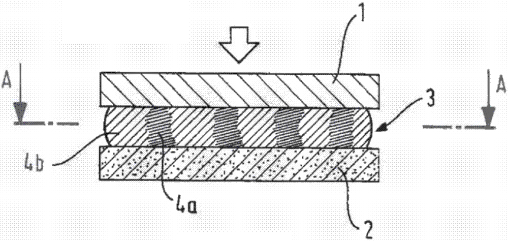
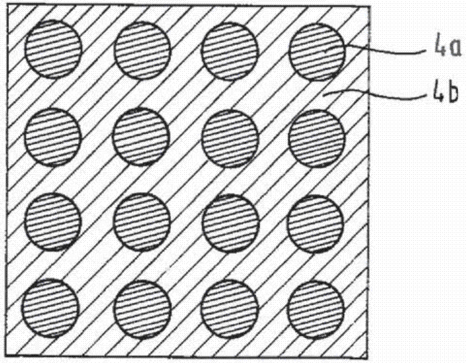
A description is given of an electronic sandwich structure which has at least a first (1) and a second part (2) to be joined, which are sintered together by means of a sintering layer (3). The sintering layer (3) is formed as a substantially uninterrupted connecting layer, the density of which varies in such a way that at least one region of higher density (4a) and at least one region of lower density (4b) alternate with one another. A description is also given of a method for forming a sintering layer (3) of an electronic sandwich structure, in which firstly a sintering material layer (3) is applied substantially continuously to a second part (2) to be joined as a connecting layer (3), this sintering material layer (3) is subsequently dried and, finally, alternating regions of higher density (4a) and of lower density (4b) of the connecting layer (3) are produced by sintering the second part to be joined (2) with the sintering layer (3) on a first part to be joined (1). The sintering material may be applied in points or stripes. The to-be-joined surfaces of the first part to be joined (1) and the second part to be joined (2) may be arranged plane-parallel, in which case the sintering layer (3) is formed with its surface regularly uneven, i.e. it has in particular regions of greater thickness (3a) and regions of smaller thickness (3b) in defined patterns, which has the effect that, after the sintering process, there are regions of higher density (4a) in the regions (3a) of thicker sintering paste application and regions of lower density (4b) in the regions (3b) of thinner sintering paste application. Alternatively, the to-be-joined surfaces of the first part to be joined (1) and the second part to be joined (2) may at least in certain regions be not arranged plane-parallel, wherein, with an initially completely uniform sintering paste application, a thinner sintering layer is obtained in the regions (4a) where the parts to be joined (1, 2) are at a smaller distance after the sintering, whereas a thicker sintering layer is formed in the regions (4b) where the distance is greater, which finally has the effect that a higher density forms in the regions (4a) where the two parts to be joined (1, 2) are at a smaller distance from one another, than in the regions (4b) where the distance between the parts to be joined (1, 2) is greater. A high lifetime of the electronic sandwich structure connected by sintering is achieved even for parts to be joined (1, 2) that have different coefficients of thermal expansion, in particular in components for power electronics.
Description
Technical field [0001] The present invention relates to an electronic sandwich structure having a first part to be joined and a second part to be joined, the first part to be joined and the second part to be joined are sintered together by means of a sintering layer. Background technique [0002] This electronic sandwich structure is used for a variety of electronic components, especially components for power electronic devices. In either case, it is necessary to ensure high current or high current density, very good heat transfer (ie, high heat flow), and reliable mechanical carrying capacity, silver sintered connections are used. For this purpose, the parts to be bonded to be sintered together are connected to each other by material bonding through a silver sintered layer, which is as uniformly thin as possible (typically having a thickness of 10 μm to 50 μm) and more or less Is compacted. In addition to the uniform layer thickness, the aim is to achieve as uniform a distribu...
Claims
Application Information
Patent Timeline
Application Date:The date an application was filed.
Publication Date:The date a patent or application was officially published.
First Publication Date:The earliest publication date of a patent with the same application number.
Issue Date:Publication date of the patent grant document.
PCT Entry Date:The Entry date of PCT National Phase.
Estimated Expiry Date:The statutory expiry date of a patent right according to the Patent Law, and it is the longest term of protection that the patent right can achieve without the termination of the patent right due to other reasons(Term extension factor has been taken into account ).
Invalid Date:Actual expiry date is based on effective date or publication date of legal transaction data of invalid patent.

