Process for transferring a layer of strained semiconductor material

a technology of donor wafers and semiconductor materials, which is applied in the direction of semiconductor devices, basic electric elements, electrical apparatus, etc., can solve the problems of reducing the switching rate of electronic components to be produced or produced, reducing the technical performance of si/sige combinations, and especially its electrical properties, and reducing the risk of complex operation of electronic components in the active part of such a combination having two on-insulator layers

Inactive Publication Date: 2005-10-11
SOITEC SA
View PDF22 Cites 57 Cited by
  • Summary
  • Abstract
  • Description
  • Claims
  • Application Information

AI Technical Summary

Benefits of technology

[0019]In the preferred embodiment, the strain imparted to the strained layer is sufficient for modifying the energy band structure of the strained layer material for improving the electrical properties thereof compared to the material in a relaxed state. The strained layer has a thickness that is sufficiently thin to prevent substantial relaxation of the strain. This thickness is preferably less than about 20 nanometers. The resulting charge carrier mobility in the strained semiconductor material layer is at least about 50% higher than in the same semiconductor material in a relaxed state.
[0021]In another embodiment, a second strained layer of a semiconductor material is provided on the first strain-retaining layer to impart the first lattice parameter therein. This enables the second strained layer to be transferred to a second receiving substrate after creating a weakened region in the first strain-retaining layer, and the first strained layer to be transferred to a first receiving substrate, such as after the transfer of the second strained layer. A second strain-retaining layer can be provided on the second strained layer substantially with the first lattice parameter for maintaining the strained state of the second strained layer from the side of the second strained layer opposite the first strain-retaining layer.

Problems solved by technology

This may substantially reduce the technical performance expected of the Si / SiGe combination, and especially its electrical properties.
Thus, for example, the SiGe layer may have a tendency to increase the circuit capacitances and therefore reduce the switching rates of the electronic components to be produced or produced in the Si / SiGe active part.
The fabrication of electronic components in the active part of such a structure comprising this combination having two on-insulator layers also has the risk of being complex to carry out, especially by the creation of lateral insulating regions in the on-insulator combination.
This process furthermore limits the application to the production of an Si / SiGe-on-insulator structure and provides no solution to the production, for example, of a strained Si-on-insulator structure.
The main objective of this process is not, however, to produce an SeOI structure with a strained silicon layer.
The silicon of the film grown epitaxially on the SiGe layer and constituting the Si layer of the final SeOI structure therefore would be little strained or unstrained, and therefore does not achieve production of a structure comprising a strained Si layer so as to benefit from its useful electrical properties, especially in SeOI structures.
Also, since the instruments for implanting species are very often limited to about 200 keV, the associated maximum implantation depths would correspond substantially to the minimum thickness of a reliable buffer layer, i.e., about one to two microns, which is insufficient to implant into the Si support substrate, so it would be difficult to use this process with an SiGe layer thick enough to contain both a buffer layer and a relaxed surface SiGe layer.
More powerful implantation instruments require an equipment infrastructure that would be very expensive and the operating costs could be prohibitive.
This type of process therefore seems to be unsuitable for producing a structure comprising a strained Si layer.
This may be prejudicial to the performance, especially the electronic performance, expected in this case of the layer of strained material, as already mentioned above.
This process furthermore limits the application to the production of such a Si / SiGe-on-insulator structure and does not provide a solution to the production, for example, of a strained Si-on-insulator structure.
This technique does make it possible to achieve thin layer thicknesses having homogeneity through the thickness, but it does entail, however, the destruction of the Si substrate and of the SiGe buffer layer by chemical etching.
These processes do not therefore afford the possibility of reusing part of the wafer, and especially at least part of the buffer layer, for a new layer transfer.
Moreover, these processes do not provide a solution to the production of a simple strained silicon-on-insulator structure.

Method used


Image

  • Process for transferring a layer of strained semiconductor material
  • Process for transferring a layer of strained semiconductor material
  • Process for transferring a layer of strained semiconductor material

Examples


Embodiment Construction

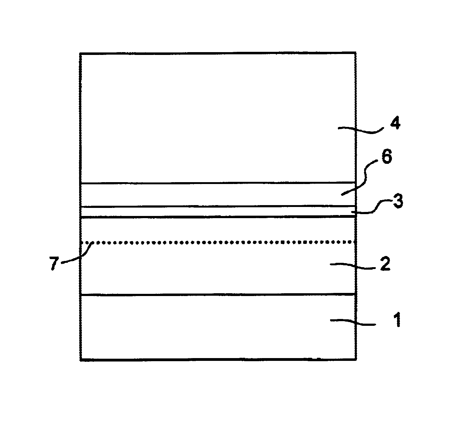
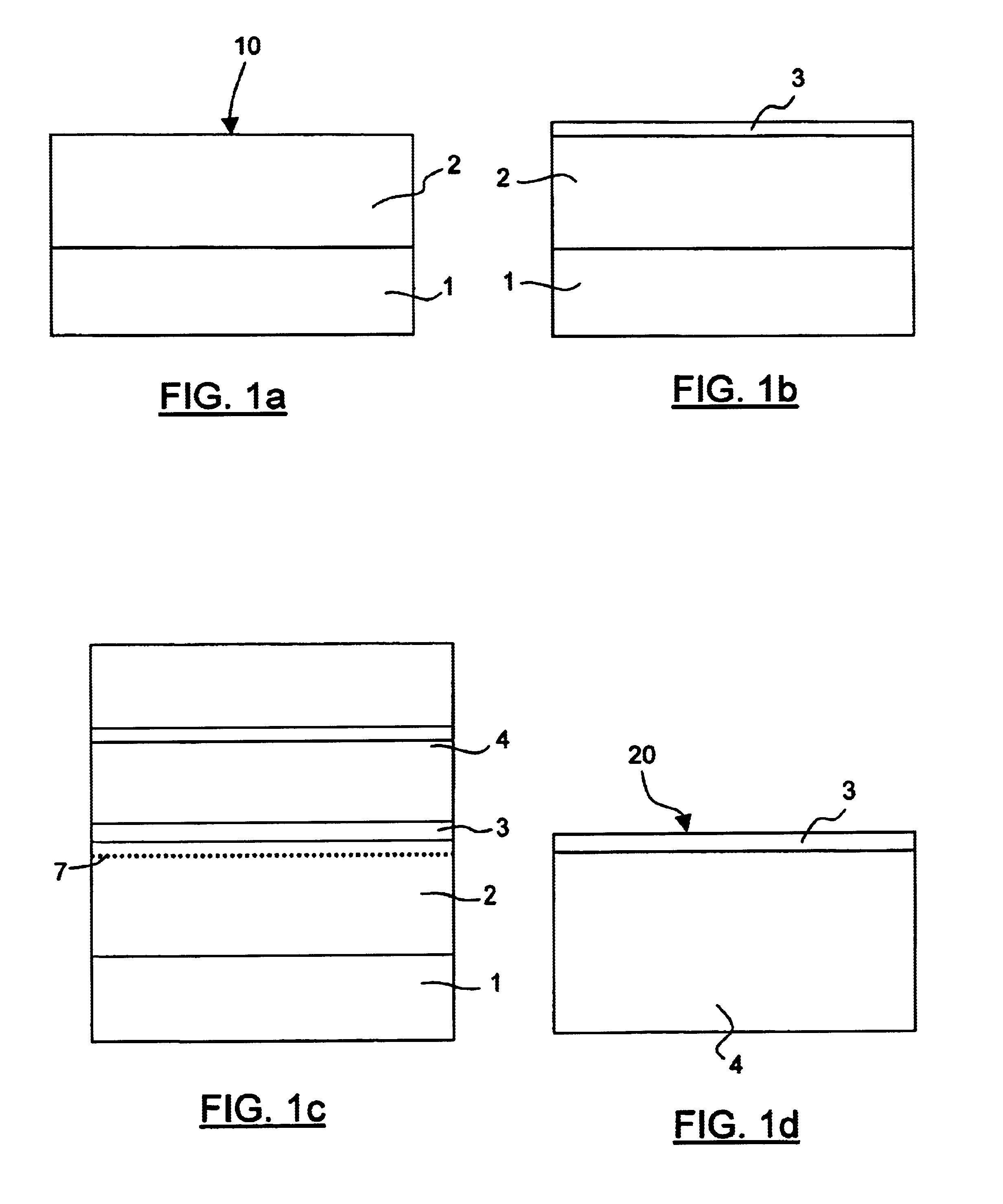
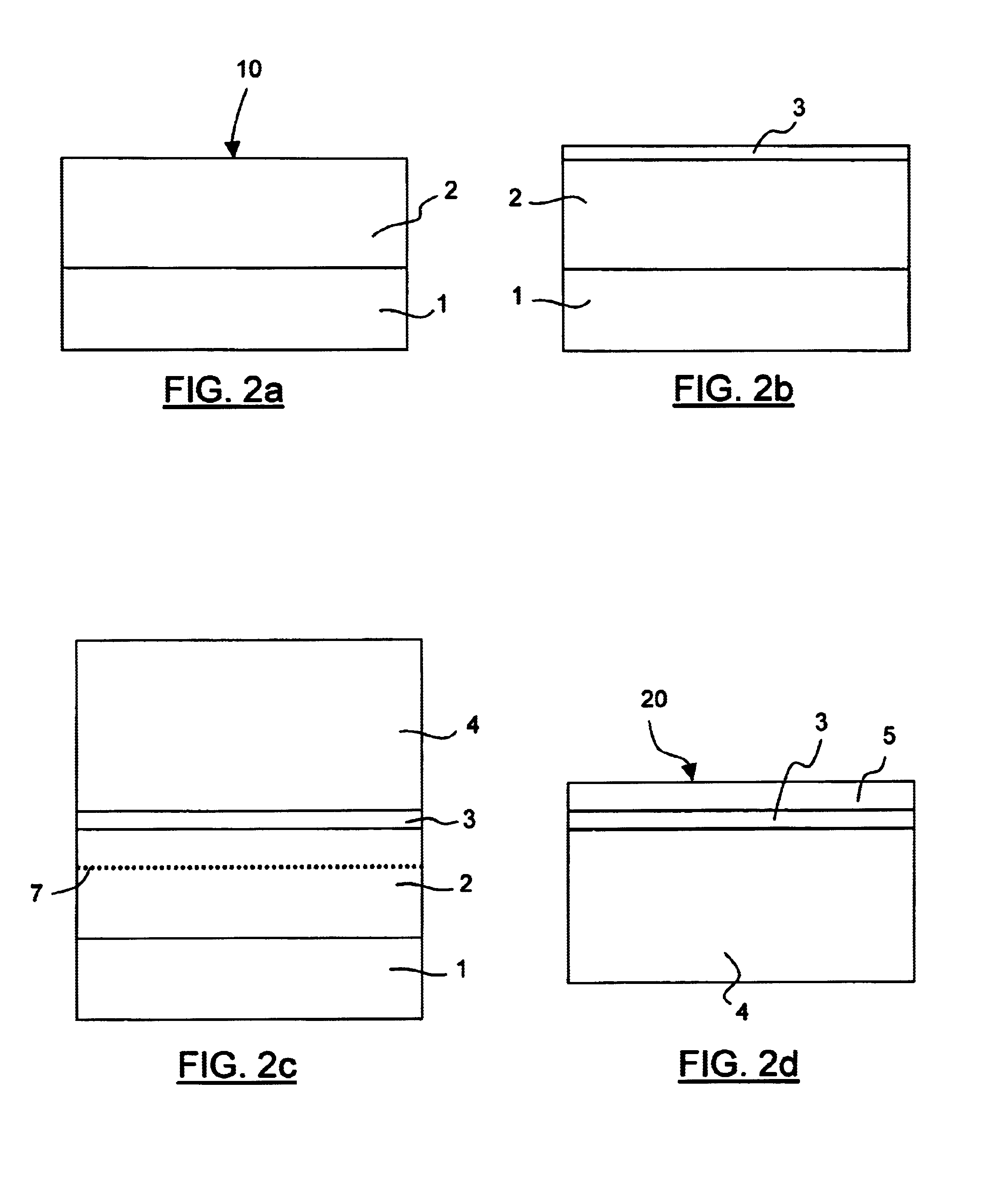
[0034]The expression “strained layer” is understood here to mean any layer of a semiconductor material with a crystallographic structure that is strained in tension or in compression during crystal growth, such as during epitaxy, with at least one lattice parameter that is substantially different from the nominal lattice parameter of this material. Conversely, the term “relaxed layer” means any layer of a semiconductor material which has an unstrained crystallographic structure. That is to say, one which has a lattice parameter substantially identical to the nominal lattice parameter of the material of the layer.

[0035]The invention aims to produce an SeOI structure. The strain exerted within the semiconductor material of the produced SeOI may in fact exhibit physical and / or electrical properties worthwhile exploiting. Thus, for example, a main benefit of tension-strained silicon layers (also called strained Si layers) consists mainly in the fact that the charge carriers (such as hol...


PUM


Abstract

The invention relates to a process for producing an electronic structure that includes a thin layer of strained semiconductor material from a donor wafer. The donor wafer has a lattice parameter matching layer that includes an upper layer of a semiconductor material having a first lattice parameter and a film of semiconductor material having a second, nominal, lattice parameter that is substantially different from the first lattice parameter and that is strained by the matching layer. This process includes transfer of the film to a receiving substrate. The invention also relates to the semiconductor structures that can be produced by the process.

Description

[0001]This application claims the benefit of provisional application No. 60 / 445,825, filed Feb. 10, 2003.FIELD OF THE INVENTION[0002]The present invention relates to the transfer of a thin layer of a donor wafer to a receiving substrate in order to form structures such as a semiconductor-on-insulator structure. The invention is aimed more particularly at carrying out this transfer in order to produce electronic structures comprising strained layers.BACKGROUND OF THE INVENTION[0003]Several processes and techniques for transferring semiconductor layers, such as Si or SiGe layers, have been proposed, in which the donor wafer comprises in succession a single-crystal silicon support substrate and a thickness of SiGe. Zhi-Yuan Cheng et al. of Massachusetts Institute of Technology has presented, in a document entitled “SiGe-On-Insulator (SGOI): Substrate Preparation and MOSFET Fabrication for Electron Mobility Evaluation” (2001 IEEE International SOI Conference, 10 / 01), two known technique...

Claims


Application Information

Patent Timeline
Patent Type & Authority Patents(United States)
IPC IPC(8): H01L21/70H01L21/762H01L29/10H01L29/02H01L21/301
CPCH01L21/76254H01L21/76259H01L29/1054Y10S438/938
Inventor GHYSELEN, BRUNOBENSAHEL, DANIELSKOTNICKI, THOMAS
Owner SOITEC SA
Why Eureka
Try Eureka