Microelectronic element with bond elements to encapsulation surface

a microelectronic element and bonding technology, applied in the field of microelectronic elements, can solve the problems of affecting the reliability and performance of the device, affecting the reliability of the device, and stressing the solder mass (or other structure)

Inactive Publication Date: 2015-03-19
INVENSAS LLC
View PDF11 Cites 60 Cited by
  • Summary
  • Abstract
  • Description
  • Claims
  • Application Information

AI Technical Summary

Benefits of technology

[0008]The first portions of the wire bonds can be encapsulated entirely by the compliant material. Further, the second portions of the wire bonds can be moveable with respect to the bases thereof. In an example, the compliant material layer can have a Young's modulus of 2.5 GPa or less.
[0009]The second portions of the wire bonds can extend along axes of the wire bonds that are disposed at angles of at least 30 degrees with respect to the third surface. The end surfaces of the wire bonds can be positioned above the third surface by a distance of at least 50 microns. Further, the end surfaces of the wire bonds can be positioned above the third surface at a distance of less than 200 microns.

Problems solved by technology

Mismatches or differences between coefficients of thermal expansion (“CTE”) of the components in such a package can adversely impact their reliability and performance.
This can cause stress in the solder masses (or other structures) used to both mount and electrically connect the semiconductor die and the substrate.
Such stress can cause the solder mass to disconnect from either or both of the semiconductor die or the substrate, thereby interrupting the signal transmission that it otherwise facilitates.
Various structures have been used to compensate for such variations in CTE, yet many fail to offer a significant amount of compensation on a scale appropriate for the fine pitch arrays being increasingly utilized in microelectronic packages.

Method used


Image

  • Microelectronic element with bond elements to encapsulation surface
  • Microelectronic element with bond elements to encapsulation surface
  • Microelectronic element with bond elements to encapsulation surface

Examples


Embodiment Construction

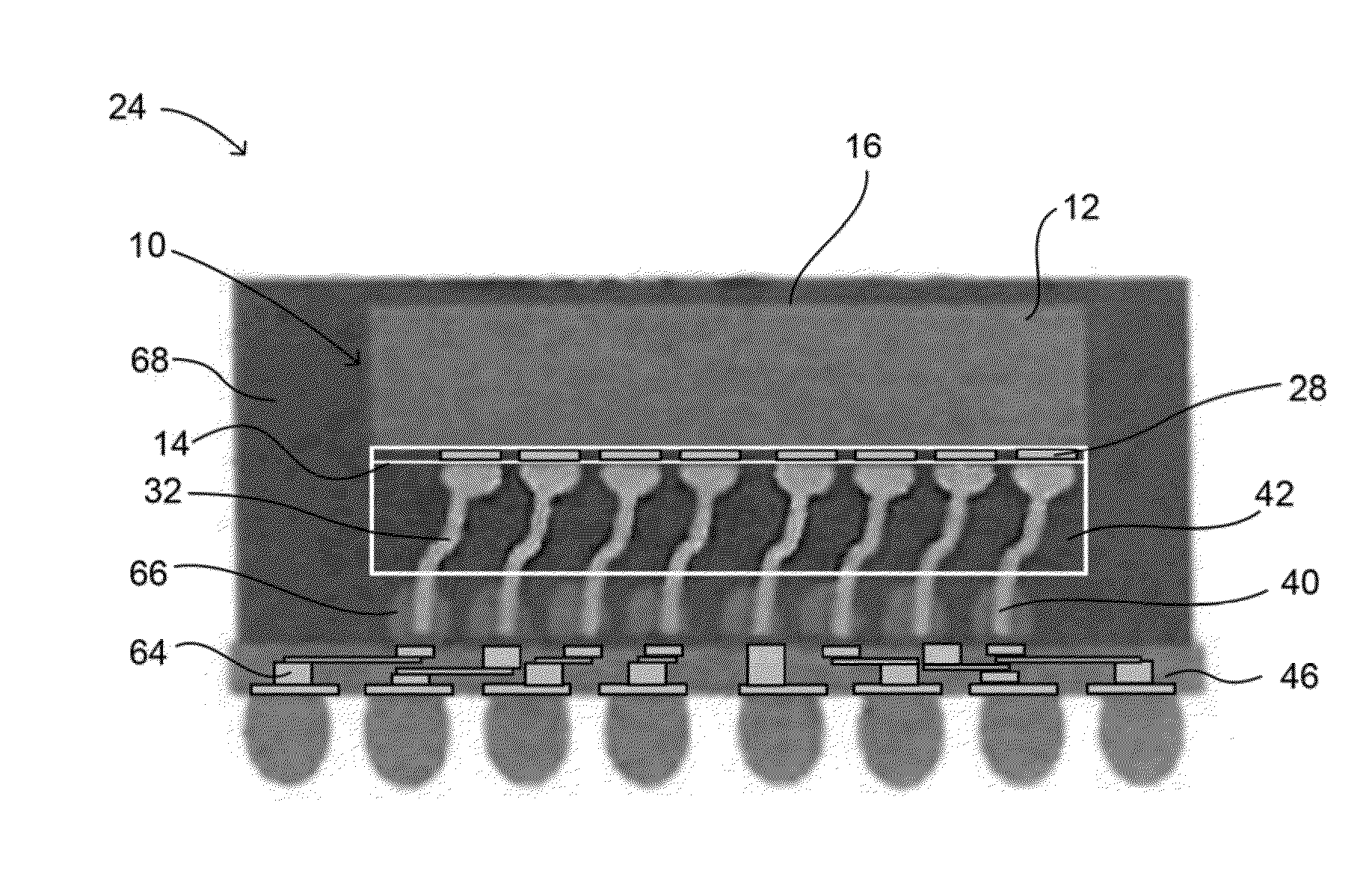
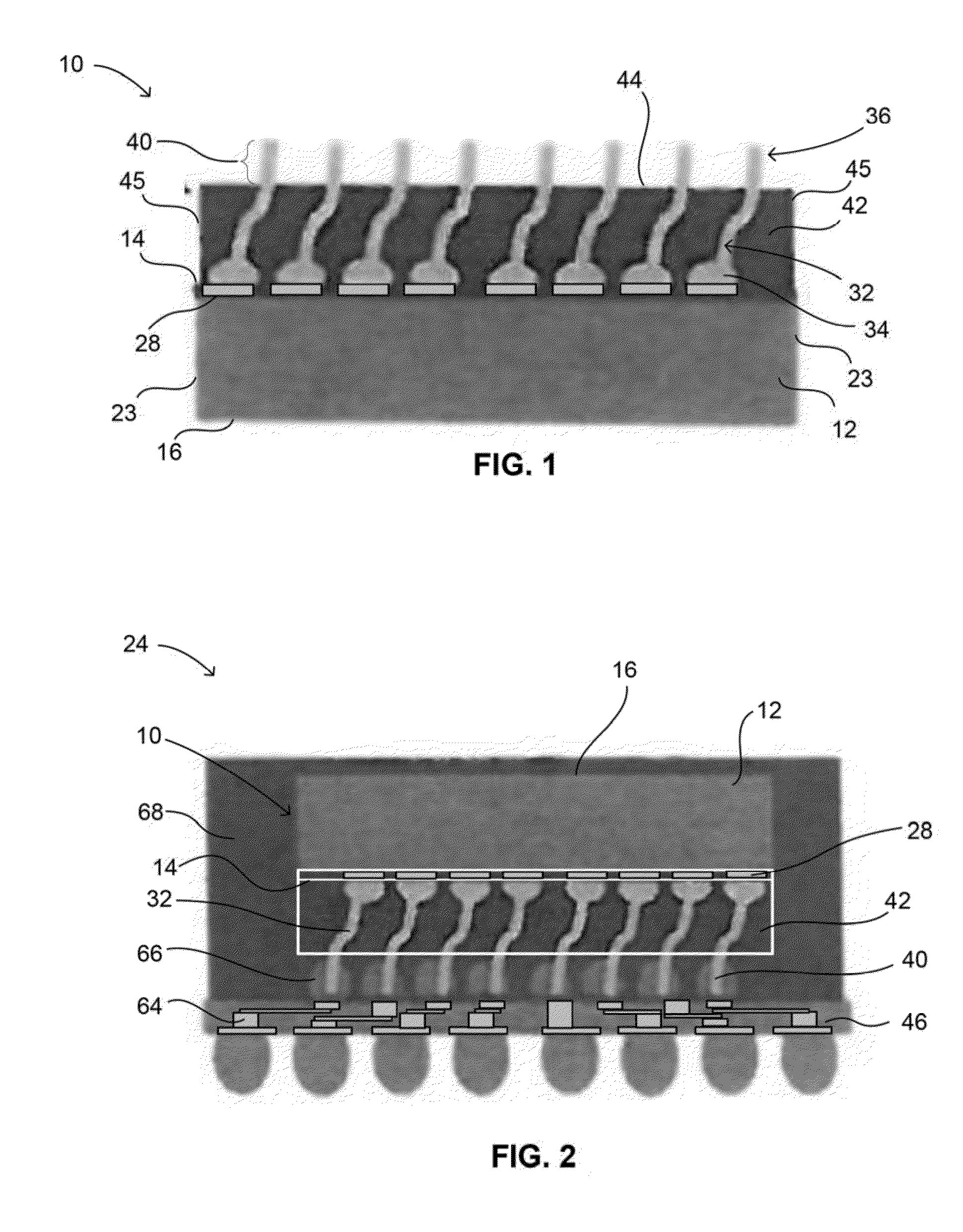
[0031]Turning now to the figures, where similar numeric references are used to indicate similar features, there is shown in FIG. 1 a microelectronic structure 10 that can be in the form of a microelectronic element according to an embodiment of the present invention. The embodiment of FIG. 1 is a microelectronic element in the form of a semiconductor die 12 (also referred to as a semiconductor chip) having a plurality of wire bonds 32 extending from contacts 28 thereof to extending portions 40 thereof that extend above a compliant material layer 42 that covers and separates remaining portions of the wire bonds 32 from each other, including portions thereof adjacent semiconductor die 12. The structure 10 can then used in computer or other electronic applications either alone or in an assembly with further components.

[0032]The microelectronic element 10 of FIG. 1 includes semiconductor die 12 having a first surface 14 and a second surface 16. For purposes of this discussion, the first...


PUM


Abstract

A microelectronic structure includes a semiconductor having conductive elements at a first surface. Wire bonds have bases joined to the conductive elements and free ends remote from the bases, the free ends being remote from the substrate and the bases and including end surfaces. The wire bonds define edge surfaces between the bases and end surfaces thereof. A compliant material layer extends along the edge surfaces within first portions of the wire bonds at least adjacent the bases thereof and fills spaces between the first portions of the wire bonds such that the first portions of the wire bonds are separated from one another by the compliant material layer. Second portions of the wire bonds are defined by the end surfaces and portions of the edge surfaces adjacent the end surfaces that are extend from a third surface of the compliant later.

Description

BACKGROUND OF THE INVENTION[0001]The subject matter of the present application relates to a microelectronic element including a semiconductor chip with structures to achieve improved reliability when assembled with external microelectronic components, including compliant connection structures, and methods of fabricating the microelectronic element.[0002]Semiconductor chips are flat bodies with contacts disposed on a front surface that are connected to internal electrical circuitry of the chip. The chips are typically packaged to form a microelectronic package having terminals that are electrically connected to the chip contacts. The terminals of the package may then be connected to an external microelectronic component, such as a circuit panel.[0003]Microelectronic devices such as semiconductor chips typically require many input and output connections to other electronic components. The input and output contacts of a semiconductor chip or other comparable device are generally dispos...

Claims


Application Information

Patent Timeline
Patent Type & Authority Applications(United States)
IPC IPC(8): H01L23/49H01L21/48
CPCH01L21/4846H01L23/49H01L2224/13076H01L2224/16105H01L2224/13005H01L2224/1369H01L2224/92143H01L2224/92142H01L23/293H01L23/3128H01L23/3171H01L21/565H01L24/11H01L24/13H01L24/16H01L24/742H01L24/745H01L24/81H01L2224/0401H01L2224/05555H01L2224/05571H01L2224/05573H01L2224/05644H01L2224/05647H01L2224/05655H01L2224/1134H01L2224/1191H01L2224/13013H01L2224/13014H01L2224/13017H01L2224/13022H01L2224/131H01L2224/13124H01L2224/13144H01L2224/13147H01L2224/13155H01L2224/1357H01L2224/13655H01L2224/14051H01L2224/16145H01L2224/16227H01L2224/1703H01L2224/17051H01L2224/32145H01L2224/73103H01L2224/73203H01L2224/73253H01L2224/742H01L2224/81191H01L2224/81193H01L2224/81815H01L2224/9202H01L2224/97H01L2224/13012H01L2224/13624H01L2224/1184H01L2224/05572H01L2224/16108H01L2224/16225H01L2924/12042H01L2225/06517H01L2225/06513H01L2225/06568H01L2924/181H01L2224/73267H01L25/0657H01L2924/00014H01L2924/014H01L2924/00012H01L2924/207H01L2224/83H01L2224/11H01L2224/81H01L2924/00H01L25/50H01L2225/06506H01L2225/06555H01L2225/06582H01L2225/06589
Inventor HABA, BELGACEMCRISP, RICHARD DEWITTZOHNI, WAEL
Owner INVENSAS LLC
Why Eureka
Try Eureka