Reconfigurable logic structures

a logic structure and reconfigurable technology, applied in the field of reconfigurable logic structures, can solve the problems of inability to alter functions, limited lifespan of anti-fuse, eeprom/fg and sonos nvm technologies, and early programmable logic device architectures,

Inactive Publication Date: 2009-03-31
CSWITCH
View PDF22 Cites 60 Cited by
  • Summary
  • Abstract
  • Description
  • Claims
  • Application Information

AI Technical Summary

Problems solved by technology

Once manufactured, these functions cannot be altered.
Early programmable logic device architectures, including the technologies used to implement their programmability, were often not up to par with their application specific integrated circuit (ASIC) counterparts.
Anti-fuse, EEPROM / FG and SONOS NVM technologies also have a limited lifespan, since they can be reprogrammed only a finite number of times; require special charge pump circuitry to generate the high voltages needed for programming; and are difficult to scale with CMOS scaling.
These drawbacks, particularly when weighed against the benefits gained by use of SRAM technology has led SRAM to become the leading programmable switch technology used in FPGAs.
Although SRAM-based programmable switch technology has become the preferred programmable switch technology, its use does present other drawbacks.
One major drawback of SRAMs is that they occupy a large percentage of the programmable fabric of an SRAM-based FPGA.
Hence, even a single 6T SRAM configuration bit occupies a significant amount of base silicon.
This problem is compounded by the fact that present day SRAM-based FPGAs can contain ten to fifty million SRAM cells.
Accordingly, SRAM-based FPGAs, although offering many benefits, have the serious drawback of the SRAM cells consuming a large portion of the FPGA chip area.
SRAMs are also susceptible to radiation-induced soft errors.
A radiation-induced soft error occurs when neutrons or alpha particles from the environment impinge on the SRAM and cause it to change state.
Finally, SRAM-based FPGAs are volatile (see FIG. 4), meaning that the SRAM-based configuration bits must be reprogrammed (i.e. reconfigured) every time the FPGA is powered down and then powered up again.
In addition to the drawback of having to wait for the FPGA to be configured to boot-up, large amounts of power are needed to complete the boot up process.
The need for special power supply and control circuitry adds further complexity and cost to systems using SRAM-based FPGAs.

Method used


Image

  • Reconfigurable logic structures
  • Reconfigurable logic structures
  • Reconfigurable logic structures

Examples


Embodiment Construction

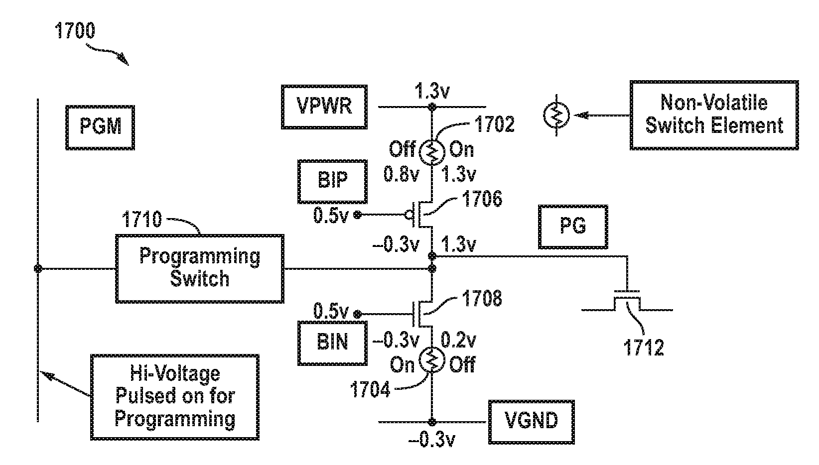
[0058]According to a first aspect of the invention, phase change material devices are used to implement programmable, non-volatile memory elements, which can be used in reconfigurable logic structures. Phase change materials (PCMs) are a class of materials that can change phase from crystalline structures to amorphous structures and vice versa when under different thermal treatments as shown in FIG. 11. When a PCM is heated above its crystallization temperature and cooled down gradually, it solidifies to a crystalline phase and exhibits low electrical resistance. However, when heated above its melting temperature and then cooled down abruptly, the PCM forms an amorphous phase and exhibits high electrical resistance. Accordingly, a PCM may be viewed as a programmable resistor having two distinct electrical resistance values as shown in FIG. 12. PCMs may contain atomic elements from Groups IV, V and VI of the periodic table of elements, such as Ge, As, Se, Te. When formed in an integr...


PUM


Abstract

Reconfigurable electronic structures and circuits using programmable, non-volatile memory elements. The programmable, non-volatile memory elements may perform the functions of storage and / or a switch to produce components such as crossbars, multiplexers, look-up tables (LUTs) and other logic circuits used in programmable logic structures (e.g., (FPGAs)). The programmable, non-volatile memory elements comprise one or more structures based on Phase Change Memory, Programmable Metallization, Carbon Nano-Electromechanical (CNT-NEM), or Metal Nano-Electromechanical device technologies.

Description

CROSS-REFERENCE TO RELATED PATENT APPLICATIONS[0001]This application relates to and incorporates by reference co-pending and commonly assigned U.S. patent application Ser. No. 11 / 267,788 entitled “Multi-Terminal Phase Change Devices” and to co-pending and commonly assigned U.S. patent application Ser. No. 11 / 267,789 entitled “Methods for Fabricating Multi-Terminal Phase Change Devices”.FIELD OF THE INVENTION[0002]The present invention relates to programmable logic devices and other programmable structures. More specifically, the present invention relates to programmable logic structures using phase change material devices and other non-volatile, reconfigurable device technologies.BACKGROUND OF THE INVENTION[0003]Digital electronic systems are comprised of essentially three different types of components: memory, microprocessor, and logic components. Memory devices store information such as, for example, the contents of a spreadsheet or database. Microprocessors execute software instr...

Claims


Application Information

Patent Timeline
Patent Type & Authority Patents(United States)
IPC IPC(8): H03K19/177G11C11/34
CPCB82Y10/00G11C13/0004G11C13/0011G11C13/025G11C23/00H03K19/17736H03K19/17748H03K19/1778
Inventor DERHARCOBIAN, NARBEHKORDUS, II, LOUIS CHARLESMURPHY, COLIN NEALOLIVA, ANTONIETTACHAN, VEI-HANSTEWART, JR., THOMAS
Owner CSWITCH
Why Eureka
Try Eureka