Integrated semiconductor circuit

A semiconductor and circuit technology, applied in the field of integrated semiconductor circuits, can solve the problems of wasting structural space and cost, and achieve the effects of small service life drift, system complexity and low balance complexity

Active Publication Date: 2017-08-29
ROBERT BOSCH GMBH
View PDF10 Cites 0 Cited by
  • Summary
  • Abstract
  • Description
  • Claims
  • Application Information

AI Technical Summary

Problems solved by technology

The disadvantage here is that the additional semiconductor area creates costs and wastes installation space

Method used


Image

  • Integrated semiconductor circuit
  • Integrated semiconductor circuit
  • Integrated semiconductor circuit

Examples


Embodiment Construction

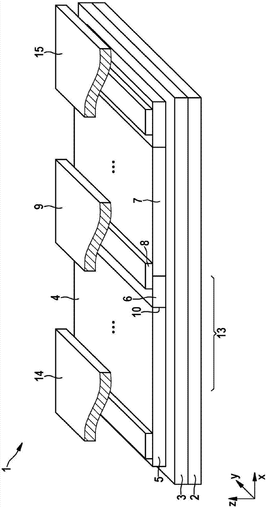
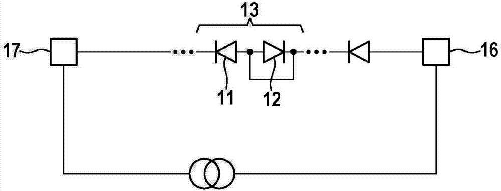
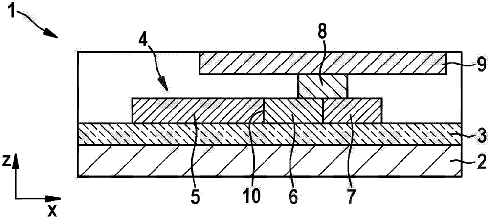
[0033] Figure 1a An integrated semiconductor circuit 1 is shown, which can be connected to other components or to voltage or current sources by means of two connection structures 14 and 15 . The integrated semiconductor circuit 1 has a planar substrate 2 on which an insulating layer 3 is arranged. A semiconductor layer 4 is arranged on the insulating layer 3 , said semiconductor layer having three mutually adjoining sections 5 , 6 and 7 . The first section 5 and the third section 7 have a first doping. The second section 6 has a second doping. The first doping and the second doping have opposite charge carriers, ie the first section 5 and the third section 7 are, for example, p-doped and the second section is n-doped. The second section 6 is arranged between the first section 5 and the third section 7 . Because the first segment 5 directly adjoins the second segment 6 and the second segment 6 directly adjoins the 7th segment, due to the opposite charge carriers of the segm...


PUM


Abstract

The invention relates to an integrated semiconductor circuit (1) with a flat substrate (2) on which an insulating layer (3) is arranged. A semiconductor layer (4) is arranged on the insulating layer (3), and the semiconductor layer (4) has at least three sections (5, 6, 7) which are directly adjacent to one another. The adjacent sections (5, 6, 7) have opposite charge carriers such that a p-n junction and an n-p junction are formed in an alternating manner. The three adjacent sections (5, 6, 7) form a diode (11) in the forward direction and a diode (12) in the reverse direction when the semiconductor layer (4) is electrically contacted. Some regions of a contact layer (8) are arranged on the sections (6, 7) which represent the diode (12) in the reverse direction such that the diode (12) is short-circuited in the reverse direction, and a metal layer (9) is arranged on the contact layer (8), wherein the metal layer (9) completely covers the contact layer (8), and at least some regions of the metal layer are vertically spaced laterally over the three adjacent sections (5, 6, 7).

Description

technical field [0001] The invention relates to an integrated semiconductor circuit, a circuit arrangement having at least two integrated semiconductor circuits, and the use of the circuit arrangement for temperature sensing. Background technique [0002] In the power output pole, for example, a predetermined temperature must not be exceeded for the operation of the electric motor. The actual temperature of the power components in the environment is not known due to manufacturing-induced numerical dispersion and operating states that cannot be determined precisely before. It is therefore known to provide buffer regions in the structure of power output stages in order to avoid temperature peaks occurring in the power components. The disadvantage here is that the additional semiconductor area creates costs and wastes installation space. [0003] Document DE 19904575 C1 describes diodes which serve as monolithically integrated temperature sensors. [0004] Document DE 10 201...

Claims


Application Information

Patent Timeline
IPC IPC(8): H01L27/02
CPCH01L27/0255
Inventor C·普伦特克W·冯埃姆登N·戴维斯
Owner ROBERT BOSCH GMBH
Why Eureka
Try Eureka