Pixel circuit, driving method, display module, driving method and display device

A technology for pixel circuits and pixels, applied in the fields of display modules, driving methods, display devices, and pixel circuits, capable of solving problems such as complex process steps and low precision

Active Publication Date: 2017-09-05
BOE TECH GRP CO LTD
View PDF9 Cites 20 Cited by
  • Summary
  • Abstract
  • Description
  • Claims
  • Application Information

AI Technical Summary

Problems solved by technology

[0003] The main purpose of the present invention is to provide a pixel circuit, a driving method, a display module, a driving method and a display device, so as to solve the problem of the existing...

Method used


Image

  • Pixel circuit, driving method, display module, driving method and display device
  • Pixel circuit, driving method, display module, driving method and display device
  • Pixel circuit, driving method, display module, driving method and display device

Examples


specific Embodiment approach

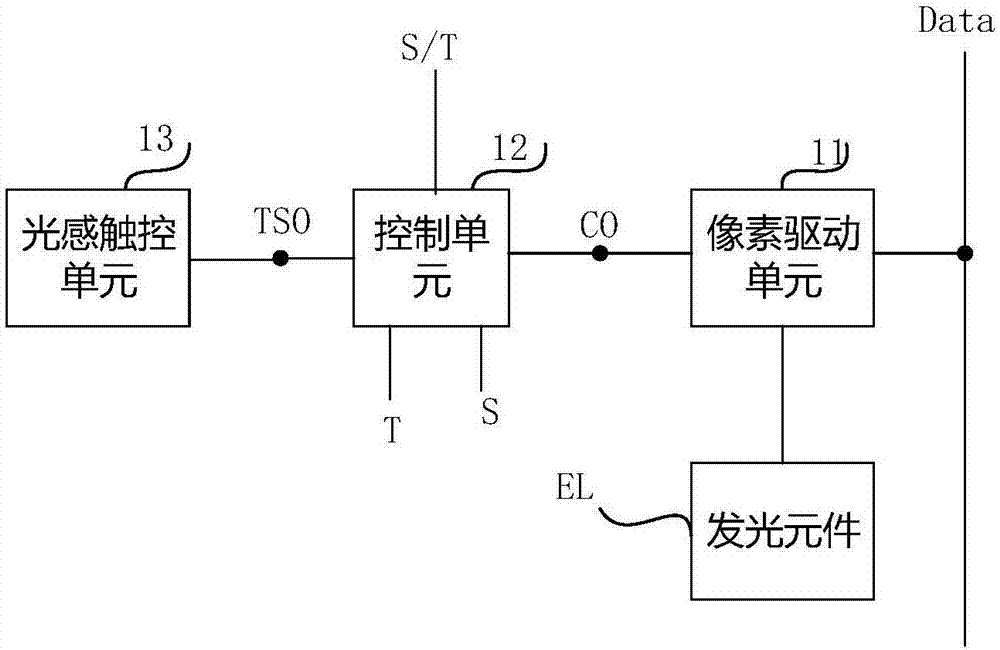
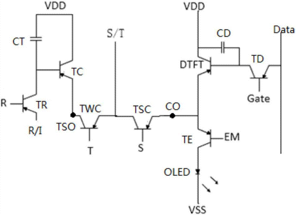
[0079] According to a specific implementation manner, the photosensitive touch unit may include a photosensitive transistor, a touch capacitor unit and a touch transistor, wherein,

[0080] The gate of the phototransistor is connected to the photoreset control terminal, the first pole of the phototransistor is connected to the first terminal of the touch capacitance unit, and the second pole of the phototransistor is connected to the photoreset signal input terminal connection;

[0081] The second end of the touch capacitor unit is connected to the first level input end;

[0082] The gate of the touch transistor is connected to the first pole of the photosensitive transistor, the first pole of the touch transistor is connected to the first level input end, the second pole of the touch transistor is connected to the The touch sensing current signal output terminal is connected.

[0083] In actual operation, the display compensation stage includes a reset time period and a pho...

Embodiment approach

[0087] According to a specific implementation manner, the pixel driving unit may include a driving transistor, a display capacitor unit, a data writing unit, and a light emission control unit, wherein,

[0088] The first end of the display capacitor unit is connected to the gate of the driving transistor, and the second end of the display capacitor unit is connected to the first electrode of the driving transistor;

[0089] The second pole of the driving transistor is connected to the compensation signal output terminal;

[0090] The data writing unit is respectively connected to the gate of the drive transistor, the corresponding row gate line and the corresponding column data line, and is used to control whether the gate of the drive transistor is connected to the corresponding column data line under the control of the corresponding row gate line. line connection;

[0091] The light emission control unit is respectively connected to the light emission control terminal, the ...


PUM


Abstract

The invention provides a pixel circuit, a driving method, a display module, a driving method and a display device. The pixel circuit comprises a touch pixel driving sub-circuit. The touch pixel driving sub-circuit comprises a pixel driving unit, a control unit and a light sensation touch unit. The light sensation touch unit outputs a touch induction current signal. The pixel driving unit is used for extracting a threshold voltage signal of driving transistors included in the pixel driving unit and outputting the threshold voltage signal. The control unit controls whether the output end of the touch induction current signal is connected with a touch display signal line or not under control of a touch reading control side and controls whether the compensating signal output end is connected with the touch display signal line or not under control of a display compensating control side. Process steps are reduced, and touch precision is high.

Description

technical field [0001] The present invention relates to the field of display technology, in particular to a pixel circuit, a driving method, a display module, a driving method and a display device. Background technique [0002] The existing AMOLED (Active-matrix organic light emitting diode, active-matrix organic light-emitting diode) display devices all use the On Cell (plug-in) capacitive touch method, which requires two independent process steps : One is a capacitive touch substrate process, and the other is an OLED (Organic LightEmitting Diode, active matrix organic light emitting diode) display substrate process. And at the same time, currently, the number of capacitive touch units is not as large as the number of display pixel units, and the function of high-precision fingerprint recognition cannot be realized. Contents of the invention [0003] The main purpose of the present invention is to provide a pixel circuit, a driving method, a display module, a driving met...

Claims


Application Information

Patent Timeline
IPC IPC(8): G09G3/3225H01L27/32G06F3/041G06F3/042
CPCG06F3/0412G06F3/042G09G3/3225H10K59/40G09G3/3233G09G3/3275G09G2320/045G06F3/0416H10K59/1213H10K59/1216
Inventor 马占洁
Owner BOE TECH GRP CO LTD
Why Eureka
Try Eureka