Array substrate and manufacturing method thereof, and display device

A technology of array substrates and substrate substrates, which is applied in semiconductor/solid-state device manufacturing, semiconductor devices, electrical components, etc., can solve the problems of high cost and long production process time, and achieve the effect of improving production efficiency and reducing process steps

Active Publication Date: 2015-03-04
SHANGHAI TIANMA MICRO ELECTRONICS CO LTD +1
View PDF5 Cites 27 Cited by
  • Summary
  • Abstract
  • Description
  • Claims
  • Application Information

AI Technical Summary

Problems solved by technology

The top-gate TFT array substrate in the prior art requires at least three metal layers: a light-shielding layer, a gate electrode layer, and a source and drain electrode lay

Method used


Image

  • Array substrate and manufacturing method thereof, and display device
  • Array substrate and manufacturing method thereof, and display device
  • Array substrate and manufacturing method thereof, and display device

Examples


Embodiment Construction

[0020] Specific embodiments of the present invention provide an array substrate, a manufacturing method thereof, and a display device, which are used to reduce process steps, thereby reducing production costs and improving production efficiency.

[0021] In order to make the purpose, technical solutions and advantages of the present invention clearer, the present invention will be further described in detail below in conjunction with the accompanying drawings. Obviously, the described embodiments are only some of the embodiments of the present invention, rather than all of them. Based on the embodiments of the present invention, all other embodiments obtained by persons of ordinary skill in the art without making creative efforts belong to the protection scope of the present invention.

[0022] A detailed introduction of the technical solutions provided by specific embodiments of the present invention is given below.

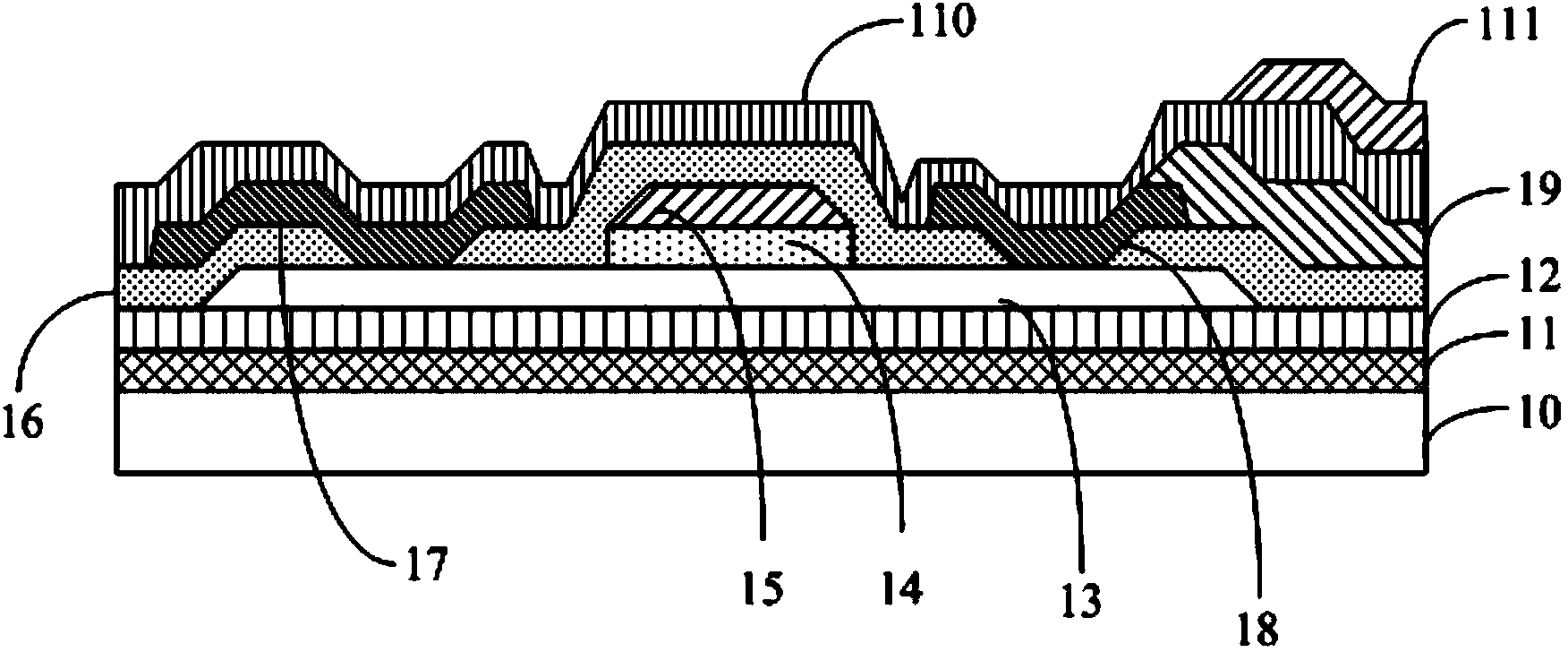
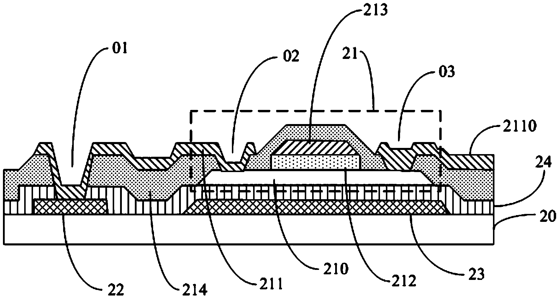
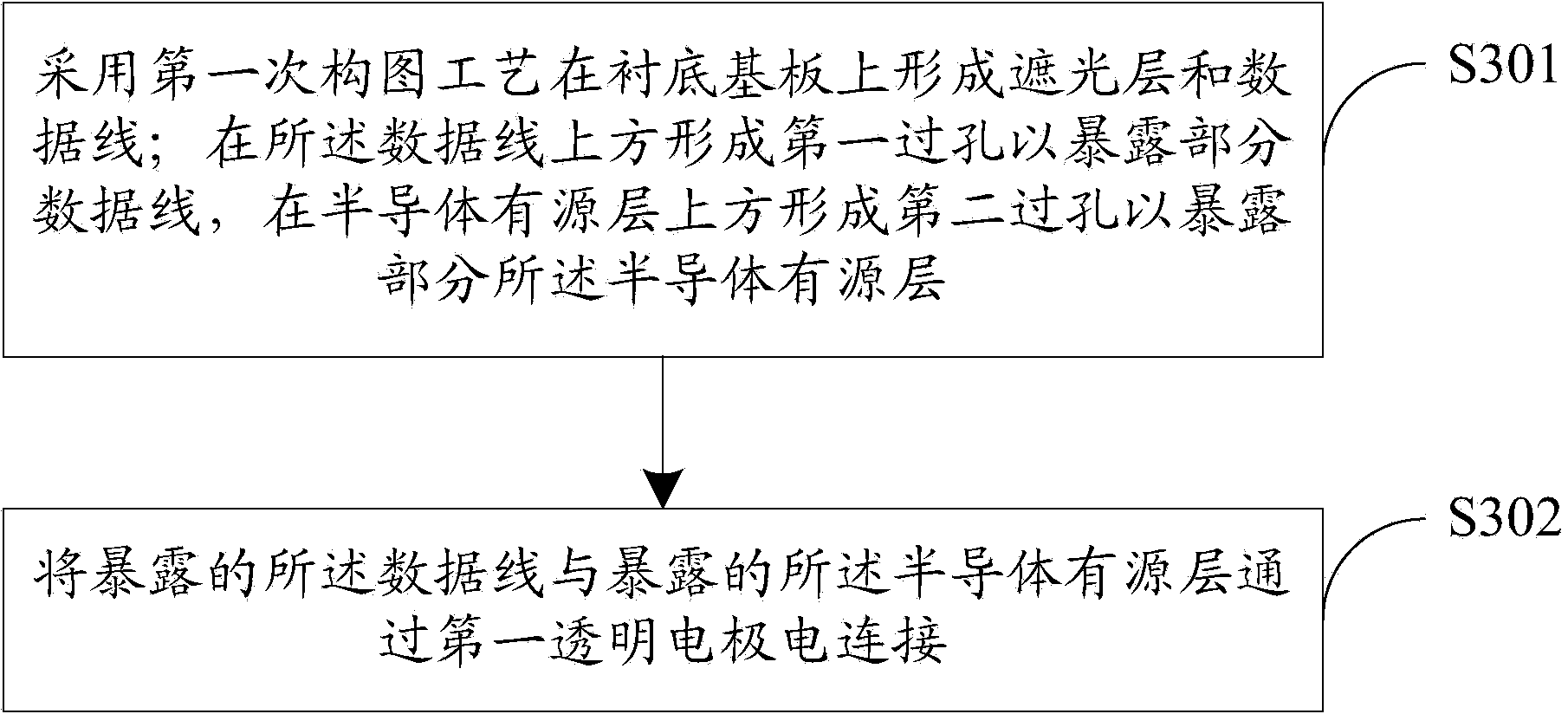
[0023] Such as figure 2 As shown, the specific embodimen...


PUM


Abstract

The invention discloses an array substrate and a manufacturing method thereof, and a display device. Therefore, the process steps are reduced, so that the production cost is lowered and the production efficiency is improved. The array substrate includes a substrate base plate, thin-film transistors arranged on the substrate base plate, data lines connected with source electrodes/drain electrodes of all thin-film transistors, and a light shield layer arranged on the substrate base plate. The data lines and the light shield layer are arranged at the same layer. First via holes are formed above the data lines to expose parts of data lines. The thin-film transistors include semiconductor active layers and first transparent electrodes; second via holes are formed above the semiconductor active layers to expose parts of the semiconductor active layers; and the data lines and the semiconductor active layers are electrically connected by the first transparent electrodes through the first via holes and the second via holes.

Description

technical field [0001] The present invention relates to the field of display technology, in particular to an array substrate, a manufacturing method thereof, and a display device. Background technique [0002] At present, thin film transistor liquid crystal display (Thin Film Transistor Liquid Crystal Display, TFT-LCD) has the advantages of small size, low power consumption, no radiation, etc., and occupies a dominant position in the current flat panel display market. Thin Film Transistor (TFT) can be divided into top gate TFT and bottom gate TFT according to its structure. Compared with the bottom-gate TFT, the top-gate TFT structure can greatly reduce the parasitic capacitance between the source-drain electrode and the gate, thereby reducing loading, reducing the size of the gate driving circuit, and further reducing the frame of the display panel. [0003] Such as figure 1 As shown, the top-gate TFT array substrate in the prior art includes: a base substrate 10, a light...

Claims


Application Information

Patent Timeline
IPC IPC(8): H01L27/12H01L21/77
Inventor 楼均辉霍思涛吴勇
Owner SHANGHAI TIANMA MICRO ELECTRONICS CO LTD
Why Eureka
Try Eureka